Unified Video Decoder (UVD, previously called Universal Video Decoder) is the name given to AMD's dedicated video decoding ASIC. There are multiple versions implementing a multitude of video codecs, such as H.264 and VC-1.
UVD was introduced with the Radeon HD 2000 Series and is integrated into some of AMD's GPUs and APUs. UVD occupies a considerable amount of the die surface at the time of its introduction [1] and is not to be confused with AMD's Video Coding Engine (VCE).
As of AMD Raven Ridge (released January 2018), UVD and VCE were succeeded by Video Core Next (VCN).
Overview
The UVD is based on an ATI Xilleon video processor, which is incorporated onto the same die as the GPU and is part of the ATI Avivo HD for hardware video decoding, along with the Advanced Video Processor (AVP). UVD, as stated by AMD, handles decoding of H.264/AVC, and VC-1 video codecs entirely in hardware.
The UVD technology is based on the Cadence Tensilica Xtensa [2] processor, [3] [4] [5] which was originally licensed by ATI Technologies Inc. in 2004. [6]
UVD/UVD+
In early versions of UVD, video post-processing is passed to the pixel shaders and OpenCL kernels. MPEG-2 decoding is not performed within UVD, but in the shader processors. The decoder meets the performance and profile requirements of Blu-ray and HD DVD, decoding H.264 bitstreams up to a bitrate of 40 Mbit/s. It has context-adaptive binary arithmetic coding (CABAC) support for H.264/AVC.
Unlike video acceleration blocks in previous generation GPUs, which demanded considerable host-CPU involvement, UVD offloads the entire video-decoder process for VC-1 and H.264 except for video post-processing, which is offloaded to the shaders. MPEG-2 decode is also supported, but the bitstream/entropy decode is not performed for MPEG-2 video in hardware.
Previously, neither ATI Radeon R520 series' ATI Avivo nor NVidia Geforce 7 series' PureVideo assisted front-end bitstream/entropy decompression in VC-1 and H.264 - the host CPU performed this work. [7] UVD handles VLC/ CAVLC/ CABAC, frequency transform, pixel prediction and inloop deblocking, but passes the post processing to the shaders. [8] Post-processing includes denoising, de-interlacing, and scaling/resizing. AMD has also stated that the UVD component being incorporated into the GPU core only occupies 4.7 mm² in area on 65 nm fabrication process node.
A variation on UVD, called UVD+, was introduced with the Radeon HD 3000 series. UVD+ support HDCP for higher resolution video streams. [9] But UVD+ was also being marketed as simply UVD.
UVD 2
The UVD saw a refresh with the release of the Radeon HD 4000 series products. The UVD 2 features full bitstream decoding of H.264/MPEG-4 AVC, VC-1, as well as iDCT level acceleration of MPEG2 video streams. Performance improvements allow dual video stream decoding and Picture-in-Picture mode. This makes UVD2 full BD-Live compliant.
The UVD 2.2 features a re-designed local memory interface and enhances the compatibility with MPEG2/H.264/VC-1 videos. However, it was marketed under the same alias as "UVD 2 Enhanced" as the "special core-logic, available in RV770 and RV730 series of GPUs, for hardware decoding of MPEG2, H.264 and VC-1 video with dual-stream decoding". The nature of UVD 2.2 being an incremental update to the UVD 2 can be accounted for this move.
UVD 3
UVD 3 adds support for additional hardware MPEG2 decoding (entropy decode), DivX and Xvid via MPEG-4 Part 2 decoding (entropy decode, inverse transform, motion compensation) and Blu-ray 3D via MVC (entropy decode, inverse transform, motion compensation, in-loop deblocking). [10] [11] along with 120 Hz stereo 3D support, [12] and is optimized to utilize less CPU processing power. UVD 3 also adds support for Blu-ray 3D stereoscopic displays.[ citation needed]
UVD 4
UVD 4 includes improved frame interpolation with H.264 decoder. [13] UVD 4.2 was introduced with the AMD Radeon Rx 200 series and Kaveri APU. "X.ORG Radeon UVD (Unified Video Decoder) Hardware-UVD4.2: KAVERI, KABINI, MULLINS, BONAIRE, HAWAII". May 2016.
UVD 5
UVD 5 was introduced with the AMD Radeon R9 285. New to UVD is full support for 4K H.264 video, up to level 5.2 (4Kp60). [14]
UVD 6
The UVD 6.0 decoder and Video Coding Engine 3.1 encoder were reported to be first used in GPUs based on GCN 3, including Radeon R9 Fury series and "Carrizo"-APUs, [15] [16] followed by AMD Radeon Rx 300 Series (Pirate Islands GPU family) and AMD Radeon Rx 400 Series (Arctic Islands GPU family). [17] The UVD version in "Fiji" and "Carrizo"-based graphics controller hardware is also announced to provide support for High Efficiency Video Coding (HEVC, H.265) hardware video decoding, up to 4K, 8-bits color (H.265 version 1, main profile); [18] [19] [20] and there is support for the 10bit-color HDR both H.265 and VP9 video codec in the AMD Radeon 400 series with UVD 6.3. [21] [22] [23]
UVD 7
The UVD 7.0 decoder and Video Coding Engine 4.0 encoder are included in the Vega-based GPUs. [24] [25] But there is still no fixed function VP9 hardware decoding. [26]
UVD 7.2
AMD's Vega20 GPU, present in the Instinct Mi50, Instinct Mi60 and Radeon VII cards, include VCE 4.1 and two UVD 7.2 instances. [27] [28]
VCN 1
Starting with the integrated graphics of the Raven Ridge APU (Ryzen 2200/2400G), the former UVD and VCE have been replaced by the new " Video Core Next" (VCN). VCN 1.0 adds full hardware decoding for the VP9 codec. [29]
Format support
| Implementation | MPEG-1 [a] |
H.262 (MPEG-2) |
H.263 (MPEG-4 ASP) |
VC-1/ WMV 9 |
H.264 (MPEG-4 AVC) [b] |
H.265 (HEVC) |
VP9 | AV1 | JPEG | Maximum resolution | Color depth | AMD Fluid Motion | ||||
|---|---|---|---|---|---|---|---|---|---|---|---|---|---|---|---|---|
| Decoding | Decoding | Decoding | Decoding | Decoding | Encoding | Decoding | Encoding | Decoding | Decoding | Encoding | Decoding | Frame interpolation | ||||
| UVD 1.0 | RV610, RV630, RV670, RV620, RV635 | No | No | No | Yes | Yes | No | No | No | No | No | No | No | 2K | 8-bit | No |
| UVD 2.0 | RS780, RS880, RV770 | |||||||||||||||
| UVD 2.2 | RV710, RV730, RV740 | |||||||||||||||
| UVD 2.3 | Cedar, Redwood, Juniper, Cypress | |||||||||||||||
| UVD 3.0 | Palm (Wrestler/Ontario), Sumo (Llano), Sumo2 (Llano) | Yes | Yes | Yes | ||||||||||||
| UVD 3.1 | Barts, Turks, Caicos, Cayman, Seymour | |||||||||||||||
| UVD 3.2 | Aruba (Trinity/Richland), Tahiti | VCE [A] | ||||||||||||||
| UVD 4.0 | Cape Verde, Pitcairn | Yes | ||||||||||||||
| UVD 4.2 | Kaveri, Kabini, Mullins, Bonaire, Hawaii | |||||||||||||||
| UVD 5.0 | Tonga | 4K | ||||||||||||||
| UVD 6.0 | Carrizo, Fiji | Yes | Yes | |||||||||||||
| UVD 6.2 | Stoney | 10-bit | ||||||||||||||
| UVD 6.3 | Polaris, VegaM, Lexa | VCE [A] | ||||||||||||||
| UVD 7.0 | Vega10, Vega12 | |||||||||||||||
| UVD 7.2 | Vega20 | |||||||||||||||
| VCN 1.0 | Raven, Picasso | Yes | Yes | Yes | ||||||||||||
| VCN 2.0 | Navi10, Navi12, Navi14, Renoir, Cézanne | 8K | No | |||||||||||||
| VCN 2.5 | Arcturus | |||||||||||||||
| VCN 2.6 | Aldebaran | |||||||||||||||
| VCN 3.0 | Navi21, Navi22, Navi23, Navi24 | Yes | ||||||||||||||
| VCN 3.1.0 | Van Gogh | ? | ? | ? | ||||||||||||
| VCN 3.1.1 | Rembrandt | No | No | No | No | 8K | 10-bit | No | ||||||||
| VCN 3.1.2 | Raphael | ? | ? | ? | ||||||||||||
| VCN 4.0 | Navi 3x | Yes | ? | ? | ? | |||||||||||
| Implementation | Decoding | Decoding | Decoding | Decoding | Decoding | Encoding | Decoding | Encoding | Decoding | Decoding | Encoding | Decoding | Maximum resolution | Color depth | Frame interpolation | |
| MPEG-1 [a] |
H.262 (MPEG-2) |
H.263 (MPEG-4 ASP) |
VC-1/ WMV 9 |
H.264 (MPEG-4 AVC) |
H.265 (HEVC) |
VP9 | AV1 | JPEG | AMD Fluid Motion | |||||||
- ^ a b MPEG-4 AVC and HEVC encoding by separate Video Coding Engine
Availability
Most of the Radeon HD 2000 series video cards implement the UVD for hardware decoding of 1080p high definition contents. [31] However, the Radeon HD 2900 series video cards do not include the UVD (though it is able to provide partial functionality through the use of its shaders), which was incorrectly stated to be present on the product pages and package boxes of the add-in partners' products before the launch of the Radeon HD 2900 XT,[ citation needed] either stating the card as featuring ATI Avivo HD or explicitly UVD,[ citation needed] which only the former statement of ATI Avivo HD is correct. The exclusion of UVD was also confirmed by AMD officials. [32]
UVD2 is implemented in the Radeon RV7x0 and R7x0 series GPUs. This also includes the RS7x0 series used for the AMD 700 chipset series IGP motherboards.
Feature overview
APUs
The following table shows features of AMD's processors with 3D graphics, including APUs (see also: List of AMD processors with 3D graphics).
| Platform | High, standard and low power | Low and ultra-low power | |||||||||||||||||||||||||||||||||||||||||||||||||||||||||||||||||||||||||||||||||||||||||||||||||||
|---|---|---|---|---|---|---|---|---|---|---|---|---|---|---|---|---|---|---|---|---|---|---|---|---|---|---|---|---|---|---|---|---|---|---|---|---|---|---|---|---|---|---|---|---|---|---|---|---|---|---|---|---|---|---|---|---|---|---|---|---|---|---|---|---|---|---|---|---|---|---|---|---|---|---|---|---|---|---|---|---|---|---|---|---|---|---|---|---|---|---|---|---|---|---|---|---|---|---|---|---|---|
| Codename | Server | Basic | Toronto | ||||||||||||||||||||||||||||||||||||||||||||||||||||||||||||||||||||||||||||||||||||||||||||||||||
| Micro | Kyoto | ||||||||||||||||||||||||||||||||||||||||||||||||||||||||||||||||||||||||||||||||||||||||||||||||||||
| Desktop | Performance | Raphael | Phoenix | ||||||||||||||||||||||||||||||||||||||||||||||||||||||||||||||||||||||||||||||||||||||||||||||||||
| Mainstream | Llano | Trinity | Richland | Kaveri | Kaveri Refresh (Godavari) | Carrizo | Bristol Ridge | Raven Ridge | Picasso | Renoir | Cezanne | ||||||||||||||||||||||||||||||||||||||||||||||||||||||||||||||||||||||||||||||||||||||||||
| Entry | |||||||||||||||||||||||||||||||||||||||||||||||||||||||||||||||||||||||||||||||||||||||||||||||||||||
| Basic | Kabini | Dalí | |||||||||||||||||||||||||||||||||||||||||||||||||||||||||||||||||||||||||||||||||||||||||||||||||||
| Mobile | Performance | Renoir | Cezanne | Rembrandt | Dragon Range | ||||||||||||||||||||||||||||||||||||||||||||||||||||||||||||||||||||||||||||||||||||||||||||||||
| Mainstream | Llano | Trinity | Richland | Kaveri | Carrizo | Bristol Ridge | Raven Ridge | Picasso |
Renoir Lucienne |
Cezanne Barceló |
Phoenix | ||||||||||||||||||||||||||||||||||||||||||||||||||||||||||||||||||||||||||||||||||||||||||
| Entry | Dalí | Mendocino | |||||||||||||||||||||||||||||||||||||||||||||||||||||||||||||||||||||||||||||||||||||||||||||||||||
| Basic | Desna, Ontario, Zacate | Kabini, Temash | Beema, Mullins | Carrizo-L | Stoney Ridge | Pollock | |||||||||||||||||||||||||||||||||||||||||||||||||||||||||||||||||||||||||||||||||||||||||||||||
| Embedded | Trinity | Bald Eagle |
Merlin Falcon, Brown Falcon |
Great Horned Owl | Grey Hawk | Ontario, Zacate | Kabini |
Steppe Eagle,
Crowned Eagle, LX-Family |
Prairie Falcon | Banded Kestrel | River Hawk | ||||||||||||||||||||||||||||||||||||||||||||||||||||||||||||||||||||||||||||||||||||||||||
| Released | Aug 2011 | Oct 2012 | Jun 2013 | Jan 2014 | 2015 | Jun 2015 | Jun 2016 | Oct 2017 | Jan 2019 | Mar 2020 | Jan 2021 | Jan 2022 | Sep 2022 | Jan 2023 | Jan 2011 | May 2013 | Apr 2014 | May 2015 | Feb 2016 | Apr 2019 | Jul 2020 | Jun 2022 | Nov 2022 | ||||||||||||||||||||||||||||||||||||||||||||||||||||||||||||||||||||||||||||||
| CPU microarchitecture | K10 | Piledriver | Steamroller | Excavator | " Excavator+" [33] | Zen | Zen+ | Zen 2 | Zen 3 | Zen 3+ | Zen 4 | Bobcat | Jaguar | Puma | Puma+ [34] | " Excavator+" | Zen | Zen+ | " Zen 2+" | ||||||||||||||||||||||||||||||||||||||||||||||||||||||||||||||||||||||||||||||||||
| ISA | x86-64 v1 | x86-64 v2 | x86-64 v3 | x86-64 v4 | x86-64 v1 | x86-64 v2 | x86-64 v3 | ||||||||||||||||||||||||||||||||||||||||||||||||||||||||||||||||||||||||||||||||||||||||||||||
| Socket | Desktop | Performance | — | AM5 | — | — | |||||||||||||||||||||||||||||||||||||||||||||||||||||||||||||||||||||||||||||||||||||||||||||||
| Mainstream | — | AM4 | — | — | |||||||||||||||||||||||||||||||||||||||||||||||||||||||||||||||||||||||||||||||||||||||||||||||||
| Entry | FM1 | FM2 | FM2+ | FM2+ [a], AM4 | AM4 | — | |||||||||||||||||||||||||||||||||||||||||||||||||||||||||||||||||||||||||||||||||||||||||||||||
| Basic | — | — | AM1 | — | FP5 | — | |||||||||||||||||||||||||||||||||||||||||||||||||||||||||||||||||||||||||||||||||||||||||||||||
| Other | FS1 | FS1+, FP2 | FP3 | FP4 | FP5 | FP6 | FP7 | FL1 | FP7 FP7r2 FP8 |
? | FT1 | FT3 | FT3b | FP4 | FP5 | FT5 | FP5 | FT6 | |||||||||||||||||||||||||||||||||||||||||||||||||||||||||||||||||||||||||||||||||||
| PCI Express version | 2.0 | 3.0 | 4.0 | 5.0 | 4.0 | 2.0 | 3.0 | ||||||||||||||||||||||||||||||||||||||||||||||||||||||||||||||||||||||||||||||||||||||||||||||
| CXL | — | — | |||||||||||||||||||||||||||||||||||||||||||||||||||||||||||||||||||||||||||||||||||||||||||||||||||
| Fab. ( nm) |
GF
32SHP ( HKMG SOI) |
GF
28SHP (HKMG bulk) |
GF
14LPP ( FinFET bulk) |
GF
12LP (FinFET bulk) |
TSMC
N7 (FinFET bulk) |
TSMC
N6 (FinFET bulk) |
CCD: TSMC
N5 (FinFET bulk) cIOD: TSMC N6 (FinFET bulk) |
TSMC
4nm (FinFET bulk) |
TSMC
N40 (bulk) |
TSMC
N28 (HKMG bulk) |
GF 28SHP (HKMG bulk) |
GF
14LPP ( FinFET bulk) |
GF
12LP (FinFET bulk) |
TSMC
N6 (FinFET bulk) | |||||||||||||||||||||||||||||||||||||||||||||||||||||||||||||||||||||||||||||||||||||||
| Die area (mm2) | 228 | 246 | 245 | 245 | 250 | 210 [35] | 156 | 180 | 210 | CCD: (2x) 70 cIOD: 122 |
178 | 75 (+ 28 FCH) | 107 | ? | 125 | 149 | ~100 | ||||||||||||||||||||||||||||||||||||||||||||||||||||||||||||||||||||||||||||||||||||
| Min TDP (W) | 35 | 17 | 12 | 10 | 15 | 105 | 35 | 4.5 | 4 | 3.95 | 10 | 6 | 12 | 8 | |||||||||||||||||||||||||||||||||||||||||||||||||||||||||||||||||||||||||||||||||||||||
| Max APU TDP (W) | 100 | 95 | 65 | 45 | 170 | 54 | 18 | 25 | 6 | 54 | 15 | ||||||||||||||||||||||||||||||||||||||||||||||||||||||||||||||||||||||||||||||||||||||||||
| Max stock APU base clock (GHz) | 3 | 3.8 | 4.1 | 4.1 | 3.7 | 3.8 | 3.6 | 3.7 | 3.8 | 4.0 | 3.3 | 4.7 | 4.3 | 1.75 | 2.2 | 2 | 2.2 | 3.2 | 2.6 | 1.2 | 3.35 | 2.8 | |||||||||||||||||||||||||||||||||||||||||||||||||||||||||||||||||||||||||||||||
| Max APUs per node [b] | 1 | 1 | |||||||||||||||||||||||||||||||||||||||||||||||||||||||||||||||||||||||||||||||||||||||||||||||||||
| Max core dies per CPU | 1 | 2 | 1 | 1 | |||||||||||||||||||||||||||||||||||||||||||||||||||||||||||||||||||||||||||||||||||||||||||||||||
| Max CCX per core die | 1 | 2 | 1 | 1 | |||||||||||||||||||||||||||||||||||||||||||||||||||||||||||||||||||||||||||||||||||||||||||||||||
| Max cores per CCX | 4 | 8 | 2 | 4 | 2 | 4 | |||||||||||||||||||||||||||||||||||||||||||||||||||||||||||||||||||||||||||||||||||||||||||||||
| Max CPU [c] cores per APU | 4 | 8 | 16 | 8 | 2 | 4 | 2 | 4 | |||||||||||||||||||||||||||||||||||||||||||||||||||||||||||||||||||||||||||||||||||||||||||||
| Max threads per CPU core | 1 | 2 | 1 | 2 | |||||||||||||||||||||||||||||||||||||||||||||||||||||||||||||||||||||||||||||||||||||||||||||||||
| Integer pipeline structure | 3+3 | 2+2 | 4+2 | 4+2+1 | 1+3+3+1+2 | 1+1+1+1 | 2+2 | 4+2 | 4+2+1 | ||||||||||||||||||||||||||||||||||||||||||||||||||||||||||||||||||||||||||||||||||||||||||||
| i386, i486, i586, CMOV, NOPL, i686, PAE, NX bit, CMPXCHG16B, AMD-V, RVI, ABM, and 64-bit LAHF/SAHF | |||||||||||||||||||||||||||||||||||||||||||||||||||||||||||||||||||||||||||||||||||||||||||||||||||||
| IOMMU [d] | — | v2 | v1 | v2 | |||||||||||||||||||||||||||||||||||||||||||||||||||||||||||||||||||||||||||||||||||||||||||||||||
| BMI1, AES-NI, CLMUL, and F16C | — | ||||||||||||||||||||||||||||||||||||||||||||||||||||||||||||||||||||||||||||||||||||||||||||||||||||
| MOVBE | — | ||||||||||||||||||||||||||||||||||||||||||||||||||||||||||||||||||||||||||||||||||||||||||||||||||||
| AVIC, BMI2, RDRAND, and MWAITX/MONITORX | — | ||||||||||||||||||||||||||||||||||||||||||||||||||||||||||||||||||||||||||||||||||||||||||||||||||||
| SME [e], TSME [e], ADX, SHA, RDSEED, SMAP, SMEP, XSAVEC, XSAVES, XRSTORS, CLFLUSHOPT, CLZERO, and PTE Coalescing | — | — | |||||||||||||||||||||||||||||||||||||||||||||||||||||||||||||||||||||||||||||||||||||||||||||||||||
| GMET, WBNOINVD, CLWB, QOS, PQE-BW, RDPID, RDPRU, and MCOMMIT | — | — | |||||||||||||||||||||||||||||||||||||||||||||||||||||||||||||||||||||||||||||||||||||||||||||||||||
| MPK, VAES | — | — | |||||||||||||||||||||||||||||||||||||||||||||||||||||||||||||||||||||||||||||||||||||||||||||||||||
| SGX | — | — | |||||||||||||||||||||||||||||||||||||||||||||||||||||||||||||||||||||||||||||||||||||||||||||||||||
| FPUs per core | 1 | 0.5 | 1 | 1 | 0.5 | 1 | |||||||||||||||||||||||||||||||||||||||||||||||||||||||||||||||||||||||||||||||||||||||||||||||
| Pipes per FPU | 2 | 2 | |||||||||||||||||||||||||||||||||||||||||||||||||||||||||||||||||||||||||||||||||||||||||||||||||||
| FPU pipe width | 128-bit | 256-bit | 80-bit | 128-bit | 256-bit | ||||||||||||||||||||||||||||||||||||||||||||||||||||||||||||||||||||||||||||||||||||||||||||||||
| CPU instruction set SIMD level | SSE4a [f] | AVX | AVX2 | AVX-512 | SSSE3 | AVX | AVX2 | ||||||||||||||||||||||||||||||||||||||||||||||||||||||||||||||||||||||||||||||||||||||||||||||
| 3DNow! | 3DNow!+ | — | — | ||||||||||||||||||||||||||||||||||||||||||||||||||||||||||||||||||||||||||||||||||||||||||||||||||
| PREFETCH/PREFETCHW | |||||||||||||||||||||||||||||||||||||||||||||||||||||||||||||||||||||||||||||||||||||||||||||||||||||
| GFNI | — | — | |||||||||||||||||||||||||||||||||||||||||||||||||||||||||||||||||||||||||||||||||||||||||||||||||||
| AMX | — | ||||||||||||||||||||||||||||||||||||||||||||||||||||||||||||||||||||||||||||||||||||||||||||||||||||
| FMA4, LWP, TBM, and XOP | — | — | — | — | |||||||||||||||||||||||||||||||||||||||||||||||||||||||||||||||||||||||||||||||||||||||||||||||||
| FMA3 | |||||||||||||||||||||||||||||||||||||||||||||||||||||||||||||||||||||||||||||||||||||||||||||||||||||
| AMD XDNA | — | — | |||||||||||||||||||||||||||||||||||||||||||||||||||||||||||||||||||||||||||||||||||||||||||||||||||
| L1 data cache per core (KiB) | 64 | 16 | 32 | 32 | |||||||||||||||||||||||||||||||||||||||||||||||||||||||||||||||||||||||||||||||||||||||||||||||||
| L1 data cache associativity (ways) | 2 | 4 | 8 | 8 | |||||||||||||||||||||||||||||||||||||||||||||||||||||||||||||||||||||||||||||||||||||||||||||||||
| L1 instruction caches per core | 1 | 0.5 | 1 | 1 | 0.5 | 1 | |||||||||||||||||||||||||||||||||||||||||||||||||||||||||||||||||||||||||||||||||||||||||||||||
| Max APU total L1 instruction cache (KiB) | 256 | 128 | 192 | 256 | 512 | 256 | 64 | 128 | 96 | 128 | |||||||||||||||||||||||||||||||||||||||||||||||||||||||||||||||||||||||||||||||||||||||||||
| L1 instruction cache associativity (ways) | 2 | 3 | 4 | 8 | 2 | 3 | 4 | 8 | |||||||||||||||||||||||||||||||||||||||||||||||||||||||||||||||||||||||||||||||||||||||||||||
| L2 caches per core | 1 | 0.5 | 1 | 1 | 0.5 | 1 | |||||||||||||||||||||||||||||||||||||||||||||||||||||||||||||||||||||||||||||||||||||||||||||||
| Max APU total L2 cache (MiB) | 4 | 2 | 4 | 16 | 1 | 2 | 1 | 2 | |||||||||||||||||||||||||||||||||||||||||||||||||||||||||||||||||||||||||||||||||||||||||||||
| L2 cache associativity (ways) | 16 | 8 | 16 | 8 | |||||||||||||||||||||||||||||||||||||||||||||||||||||||||||||||||||||||||||||||||||||||||||||||||
| Max on--die L3 cache per CCX (MiB) | — | 4 | 16 | 32 | — | 4 | |||||||||||||||||||||||||||||||||||||||||||||||||||||||||||||||||||||||||||||||||||||||||||||||
| Max 3D V-Cache per CCD (MiB) | — | 64 | — | — | |||||||||||||||||||||||||||||||||||||||||||||||||||||||||||||||||||||||||||||||||||||||||||||||||
| Max total in-CCD L3 cache per APU (MiB) | 4 | 8 | 16 | 64 | 4 | ||||||||||||||||||||||||||||||||||||||||||||||||||||||||||||||||||||||||||||||||||||||||||||||||
| Max. total 3D V-Cache per APU (MiB) | — | 64 | — | — | |||||||||||||||||||||||||||||||||||||||||||||||||||||||||||||||||||||||||||||||||||||||||||||||||
| Max. board L3 cache per APU (MiB) | — | — | |||||||||||||||||||||||||||||||||||||||||||||||||||||||||||||||||||||||||||||||||||||||||||||||||||
| Max total L3 cache per APU (MiB) | 4 | 8 | 16 | 128 | 4 | ||||||||||||||||||||||||||||||||||||||||||||||||||||||||||||||||||||||||||||||||||||||||||||||||
| APU L3 cache associativity (ways) | 16 | 16 | |||||||||||||||||||||||||||||||||||||||||||||||||||||||||||||||||||||||||||||||||||||||||||||||||||
| L3 cache scheme | Victim | Victim | |||||||||||||||||||||||||||||||||||||||||||||||||||||||||||||||||||||||||||||||||||||||||||||||||||
| Max. L4 cache | — | — | |||||||||||||||||||||||||||||||||||||||||||||||||||||||||||||||||||||||||||||||||||||||||||||||||||
| Max stock DRAM support | DDR3-1866 | DDR3-2133 | DDR3-2133, DDR4-2400 | DDR4-2400 | DDR4-2933 | DDR4-3200, LPDDR4-4266 | DDR5-4800, LPDDR5-6400 | DDR5-5200 | DDR5-5600, LPDDR5x-7500 | DDR3L-1333 | DDR3L-1600 | DDR3L-1866 | DDR3-1866, DDR4-2400 | DDR4-2400 | DDR4-1600 | DDR4-3200 | LPDDR5-5500 | ||||||||||||||||||||||||||||||||||||||||||||||||||||||||||||||||||||||||||||||||||||
| Max DRAM channels per APU | 2 | 1 | 2 | 1 | 2 | ||||||||||||||||||||||||||||||||||||||||||||||||||||||||||||||||||||||||||||||||||||||||||||||||
| Max stock DRAM bandwidth (GB/s) per APU | 29.866 | 34.132 | 38.400 | 46.932 | 68.256 | 102.400 | 83.200 | 120.000 | 10.666 | 12.800 | 14.933 | 19.200 | 38.400 | 12.800 | 51.200 | 88.000 | |||||||||||||||||||||||||||||||||||||||||||||||||||||||||||||||||||||||||||||||||||||
| GPU microarchitecture | TeraScale 2 (VLIW5) | TeraScale 3 (VLIW4) | GCN 2nd gen | GCN 3rd gen | GCN 5th gen [36] | RDNA 2 | RDNA 3 | TeraScale 2 (VLIW5) | GCN 2nd gen | GCN 3rd gen [36] | GCN 5th gen | RDNA 2 | |||||||||||||||||||||||||||||||||||||||||||||||||||||||||||||||||||||||||||||||||||||||||
| GPU instruction set | TeraScale instruction set | GCN instruction set | RDNA instruction set | TeraScale instruction set | GCN instruction set | RDNA instruction set | |||||||||||||||||||||||||||||||||||||||||||||||||||||||||||||||||||||||||||||||||||||||||||||||
| Max stock GPU base clock (MHz) | 600 | 800 | 844 | 866 | 1108 | 1250 | 1400 | 2100 | 2400 | 400 | 538 | 600 | ? | 847 | 900 | 1200 | 600 | 1300 | 1900 | ||||||||||||||||||||||||||||||||||||||||||||||||||||||||||||||||||||||||||||||||||
| Max stock GPU base GFLOPS [g] | 480 | 614.4 | 648.1 | 886.7 | 1134.5 | 1760 | 1971.2 | 2150.4 | 3686.4 | 102.4 | 86 | ? | ? | ? | 345.6 | 460.8 | 230.4 | 1331.2 | 486.4 | ||||||||||||||||||||||||||||||||||||||||||||||||||||||||||||||||||||||||||||||||||
| 3D engine [h] | Up to 400:20:8 | Up to 384:24:6 | Up to 512:32:8 | Up to 704:44:16 [37] | Up to 512:32:8 | 768:48:8 | 128:8:4 | 80:8:4 | 128:8:4 | Up to 192:12:8 | Up to 192:12:4 | 192:12:4 | Up to 512:?:? | 128:?:? | |||||||||||||||||||||||||||||||||||||||||||||||||||||||||||||||||||||||||||||||||||||||
| IOMMUv1 | IOMMUv2 | IOMMUv1 | ? | IOMMUv2 | |||||||||||||||||||||||||||||||||||||||||||||||||||||||||||||||||||||||||||||||||||||||||||||||||
| Video decoder | UVD 3.0 | UVD 4.2 | UVD 6.0 | VCN 1.0 [38] | VCN 2.1 [39] | VCN 2.2 [39] | VCN 3.1 | ? | UVD 3.0 | UVD 4.0 | UVD 4.2 | UVD 6.0 | UVD 6.3 | VCN 1.0 | VCN 3.1 | ||||||||||||||||||||||||||||||||||||||||||||||||||||||||||||||||||||||||||||||||||||||
| Video encoder | — | VCE 1.0 | VCE 2.0 | VCE 3.1 | — | VCE 2.0 | VCE 3.1 | ||||||||||||||||||||||||||||||||||||||||||||||||||||||||||||||||||||||||||||||||||||||||||||||
| AMD Fluid Motion | |||||||||||||||||||||||||||||||||||||||||||||||||||||||||||||||||||||||||||||||||||||||||||||||||||||
| GPU power saving | PowerPlay | PowerTune | PowerPlay | PowerTune [40] | |||||||||||||||||||||||||||||||||||||||||||||||||||||||||||||||||||||||||||||||||||||||||||||||||
| TrueAudio | — | ? | — | ||||||||||||||||||||||||||||||||||||||||||||||||||||||||||||||||||||||||||||||||||||||||||||||||||
| FreeSync | 1 2 |
1 2 | |||||||||||||||||||||||||||||||||||||||||||||||||||||||||||||||||||||||||||||||||||||||||||||||||||
| HDCP [i] | ? | 1.4 | 2.2 | 2.3 | ? | 1.4 | 2.2 | 2.3 | |||||||||||||||||||||||||||||||||||||||||||||||||||||||||||||||||||||||||||||||||||||||||||||
| PlayReady [i] | — | 3.0 not yet | — | 3.0 not yet | |||||||||||||||||||||||||||||||||||||||||||||||||||||||||||||||||||||||||||||||||||||||||||||||||
| Supported displays [j] | 2–3 | 2–4 | 3 | 3 (desktop) 4 (mobile, embedded) |
4 | 2 | 3 | 4 | 4 | ||||||||||||||||||||||||||||||||||||||||||||||||||||||||||||||||||||||||||||||||||||||||||||
/drm/radeon
[k]
[43]
[44] |
— | — | |||||||||||||||||||||||||||||||||||||||||||||||||||||||||||||||||||||||||||||||||||||||||||||||||||
/drm/amdgpu
[k]
[45] |
— | — | |||||||||||||||||||||||||||||||||||||||||||||||||||||||||||||||||||||||||||||||||||||||||||||||||||
- ^ For FM2+ Excavator models: A8-7680, A6-7480 & Athlon X4 845.
- ^ A PC would be one node.
- ^ An APU combines a CPU and a GPU. Both have cores.
- ^ Requires firmware support.
- ^ a b Requires firmware support.
- ^ No SSE4. No SSSE3.
- ^ Single-precision performance is calculated from the base (or boost) core clock speed based on a FMA operation.
- ^ Unified shaders : texture mapping units : render output units
- ^ a b To play protected video content, it also requires card, operating system, driver, and application support. A compatible HDCP display is also needed for this. HDCP is mandatory for the output of certain audio formats, placing additional constraints on the multimedia setup.
- ^ To feed more than two displays, the additional panels must have native DisplayPort support. [42] Alternatively active DisplayPort-to-DVI/HDMI/VGA adapters can be employed.
- ^ a b DRM ( Direct Rendering Manager) is a component of the Linux kernel. Support in this table refers to the most current version.
GPUs
The following table shows features of AMD/ ATI's GPUs (see also: List of AMD graphics processing units).
| Name of GPU series | Wonder | Mach | 3D Rage | Rage Pro | Rage 128 | R100 | R200 | R300 | R400 | R500 | R600 | RV670 | R700 | Evergreen |
Northern Islands |
Southern Islands |
Sea Islands |
Volcanic Islands |
Arctic Islands/ Polaris |
Vega | Navi 1x | Navi 2x | Navi 3x | |||
|---|---|---|---|---|---|---|---|---|---|---|---|---|---|---|---|---|---|---|---|---|---|---|---|---|---|---|
| Released | 1986 | 1991 | Apr 1996 |
Mar 1997 |
Aug 1998 |
Apr 2000 |
Aug 2001 |
Sep 2002 |
May 2004 |
Oct 2005 |
May 2007 |
Nov 2007 |
Jun 2008 |
Sep 2009 |
Oct 2010 |
Jan 2012 |
Sep 2013 |
Jun 2015 |
Jun 2016, Apr 2017, Aug 2019 | Jun 2017, Feb 2019 | Jul 2019 |
Nov 2020 |
Dec 2022 | |||
| Marketing Name | Wonder | Mach | 3D Rage |
Rage Pro |
Rage 128 |
Radeon 7000 |
Radeon 8000 |
Radeon 9000 |
Radeon X700/X800 |
Radeon X1000 |
Radeon HD 2000 |
Radeon HD 3000 |
Radeon HD 4000 |
Radeon HD 5000 |
Radeon HD 6000 |
Radeon HD 7000 |
Radeon 200 |
Radeon 300 |
Radeon 400/500/600 |
Radeon RX Vega, Radeon VII |
Radeon RX 5000 |
Radeon RX 6000 |
Radeon RX 7000 | |||
| AMD support | ||||||||||||||||||||||||||
| Kind | 2D | 3D | ||||||||||||||||||||||||
| Instruction set architecture | Not publicly known | TeraScale instruction set | GCN instruction set | RDNA instruction set | ||||||||||||||||||||||
| Microarchitecture |
TeraScale 1 (VLIW) |
TeraScale 2 (VLIW5) |
|
GCN 1st gen |
GCN 2nd gen |
GCN 3rd gen |
GCN 4th gen |
GCN 5th gen |
RDNA | RDNA 2 | RDNA 3 | |||||||||||||||
| Type | Fixed pipeline [a] | Programmable pixel & vertex pipelines | Unified shader model | |||||||||||||||||||||||
| Direct3D | — | 5.0 | 6.0 | 7.0 | 8.1 | 9.0 11 ( 9_2) |
9.0b 11 ( 9_2) |
9.0c 11 ( 9_3) |
10.0 11 ( 10_0) |
10.1 11 ( 10_1) |
11 ( 11_0) | 11 (
11_1) 12 ( 11_1) |
11 (
12_0) 12 ( 12_0) |
11 (
12_1) 12 ( 12_1) |
11 (
12_1) 12 ( 12_2) | |||||||||||
| Shader model | — | 1.4 | 2.0+ | 2.0b | 3.0 | 4.0 | 4.1 | 5.0 | 5.1 | 5.1 6.5 |
6.7 | |||||||||||||||
| OpenGL | — | 1.1 | 1.2 | 1.3 | 2.1 [b] [49] | 3.3 | 4.5 (on Linux: 4.5 (Mesa 3D 21.0)) [50] [51] [52] [c] | 4.6 (on Linux: 4.6 (Mesa 3D 20.0)) | ||||||||||||||||||
| Vulkan | — | 1.0 ( Win 7+ or Mesa 17+) |
1.2 (Adrenalin 20.1.2, Linux Mesa 3D 20.0) 1.3 (GCN 4 and above (with Adrenalin 22.1.2, Mesa 22.0)) |
1.3 | ||||||||||||||||||||||
| OpenCL | — | Close to Metal | 1.1 (no Mesa 3D support) | 1.2+ (on Linux: 1.1+ (no Image support on clover, with by rustiCL) with Mesa 3D, 1.2+ on GCN 1.Gen) | 2.0+ (Adrenalin driver on
Win7+) (on Linux ROCM, Linux Mesa 3D 1.2+ (no Image support in clover, but in rustiCL with Mesa 3D, 2.0+ and 3.0 with AMD drivers or AMD ROCm), 5th gen: 2.2 win 10+ and Linux RocM 5.0+ |
2.2+ and 3.0 windows 8.1+ and Linux ROCM 5.0+ (Mesa 3D rustiCL 1.2+ and 3.0 (2.1+ and 2.2+ wip)) [53] [54] [55] | ||||||||||||||||||||
| HSA / ROCm | — | ? | ||||||||||||||||||||||||
| Video decoding ASIC | — | Avivo/ UVD | UVD+ | UVD 2 | UVD 2.2 | UVD 3 | UVD 4 | UVD 4.2 | UVD 5.0 or 6.0 | UVD 6.3 | UVD 7 [24] [d] | VCN 2.0 [24] [d] | VCN 3.0 [56] | VCN 4.0 | ||||||||||||
| Video encoding ASIC | — | VCE 1.0 | VCE 2.0 | VCE 3.0 or 3.1 | VCE 3.4 | VCE 4.0 [24] [d] | ||||||||||||||||||||
| Fluid Motion [e] | ? | |||||||||||||||||||||||||
| Power saving | ? | PowerPlay | PowerTune | PowerTune & ZeroCore Power | ? | |||||||||||||||||||||
| TrueAudio | — | Via dedicated DSP | Via shaders | |||||||||||||||||||||||
| FreeSync | — | 1 2 | ||||||||||||||||||||||||
| HDCP [f] | ? | 1.4 | 2.2 | 2.3 [57] | ||||||||||||||||||||||
| PlayReady [f] | — | 3.0 | 3.0 | |||||||||||||||||||||||
| Supported displays [g] | 1–2 | 2 | 2–6 | ? | ||||||||||||||||||||||
| Max. resolution | ? | 2–6 × 2560×1600 |
2–6 × 4096×2160 @ 30 Hz |
2–6 × 5120×2880 @ 60 Hz |
3 × 7680×4320 @ 60 Hz [58] |
7680×4320 @ 60 Hz PowerColor |
7680x4320
@165 HZ | |||||||||||||||||||
/drm/radeon
[h]
|
— | |||||||||||||||||||||||||
/drm/amdgpu
[h]
|
— | Experimental [59] | Optional [60] | |||||||||||||||||||||||
- ^ The Radeon 100 Series has programmable pixel shaders, but do not fully comply with DirectX 8 or Pixel Shader 1.0. See article on R100's pixel shaders.
- ^ R300, R400 and R500 based cards do not fully comply with OpenGL 2+ as the hardware does not support all types of non-power of two (NPOT) textures.
- ^ OpenGL 4+ compliance requires supporting FP64 shaders and these are emulated on some TeraScale chips using 32-bit hardware.
- ^ a b c The UVD and VCE were replaced by the Video Core Next (VCN) ASIC in the Raven Ridge APU implementation of Vega.
- ^ Video processing for video frame rate interpolation technique. In Windows it works as a DirectShow filter in your player. In Linux, there is no support on the part of drivers and / or community.
- ^ a b To play protected video content, it also requires card, operating system, driver, and application support. A compatible HDCP display is also needed for this. HDCP is mandatory for the output of certain audio formats, placing additional constraints on the multimedia setup.
- ^ More displays may be supported with native DisplayPort connections, or splitting the maximum resolution between multiple monitors with active converters.
- ^ a b DRM ( Direct Rendering Manager) is a component of the Linux kernel. AMDgpu is the Linux kernel module. Support in this table refers to the most current version.
Operating system support
The UVD SIP core needs to be supported by the device driver, which provides one or more interfaces such as VDPAU, VAAPI or DXVA. One of these interfaces is then used by end-user software, for example VLC media player or GStreamer, to access the UVD hardware and make use of it.
AMD Catalyst, AMD's proprietary graphics device driver that supports UVD, is available for Microsoft Windows and some Linux distributions. Additionally, a free device driver is available, which also supports the UVD hardware.
Linux

Support for UVD has been available in AMD's proprietary driver Catalyst version 8.10 since October 2008 through X-Video Motion Compensation (XvMC) or X-Video Bitstream Acceleration (XvBA). [62] [63] Since April 2013, [64] UVD is supported by the free and open-source "radeon" device driver through Video Decode and Presentation API for Unix (VDPAU). An implementation of VDPAU is available as Gallium3D state tracker in Mesa 3D.
On 28 June 2014, Phoronix published some benchmarks on using Unified Video Decoder through the VDPAU interface running MPlayer on Ubuntu 14.04 with version 10.3-testing of Mesa 3D. [65]
Windows
Microsoft Windows supported UVD since it was launched. UVD currently only supports DXVA (DirectX Video Acceleration) API specification for the Microsoft Windows and Xbox 360 platforms to allow video decoding to be hardware accelerated, thus the media player software also has to support DXVA to be able to utilize UVD hardware acceleration.
Others
Support for running custom FreeRTOS-based firmware on the Radeon HD 2400's UVD core (based on an Xtensa CPU), interfaced with a STM32 ARM-based board via I2C, was attempted as of January 2012. [66]
Predecessors and Successor
Predecessors
The Video Shader and ATI Avivo are similar technologies incorporated into previous ATI products.
Successor
The UVD was succeeded by AMD Video Core Next in the Raven Ridge series of APUs released in October 2017. The VCN combines both encode (VCE) and decode (UVD). [67]
See also
Video hardware technologies
Nvidia
- PureVideo - Nvidia
- GeForce 256's Motion Compensation
- High-Definition Video Processor
- Video Processing Engine
- Nvidia NVENC
- Nvidia NVDEC
AMD
- Video Core Next - AMD
- Video Coding Engine - AMD
- Unified Video Decoder - AMD
- Video Shader - ATI
Intel
Qualcomm
Others
- VDPAU – Video Decode and Presentation API for Unix, from NVIDIA
- Video Acceleration API (VA API) – an alternative video acceleration API to XvBA for Linux/UNIX operating-system that supports XvBA as a backend
- X-Video Bitstream Acceleration (XvBA) – AMD's future hardware acceleration API for Linux/UNIX operating-system.
- Bit stream decoder (BSD)
- Comparison of AMD graphics processing units
- DirectX Video Acceleration (DxVA) – Microsoft's hardware acceleration API for Microsoft Windows based operating-system.
Notes
References
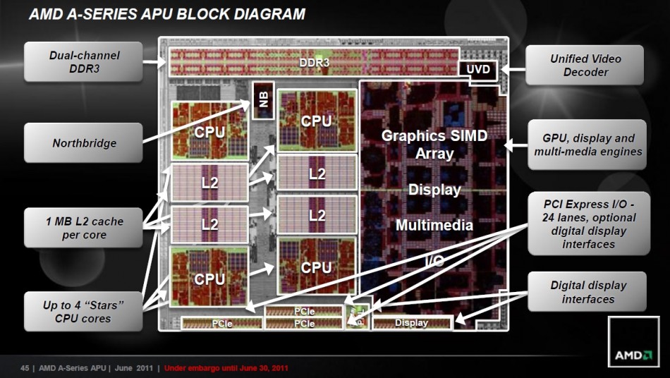
- ^ "AMD A-Series APU block diagram". 2011-06-30. Retrieved 2015-01-22.
- ^ "Linux operating system on Xtensa processors".
- ^ Cheung, Ken (2009-01-08). "Consumer Electronics Show Features Tensilica-enabled Products". EDA Geek. Archived from the original on 2014-04-26. Retrieved 2014-05-15.
- ^ "Customer Profiles | Cadence IP". Ip.cadence.com. 2014-04-13. Retrieved 2014-05-15.
- ^ "Tensilica News: Excellent AMD ATI Video with Xtensa". tensilica.com. 2009-10-05. Retrieved 2014-05-15.
- ^ "ATI Licenses Tensilica's Xtensa Configurable Processor" (Press release). Business Wire. 2004-10-18. Retrieved 2014-05-15.
- ^ "HardSpell review" (in Chinese). Archived from the original on September 27, 2007.
-
^ Smith, Ryan (February 24, 2010).
"AMD's Radeon HD 5450: The Next Step In HTPC Video Cards".
AnandTech. AnandTech, Inc. p. 4. Retrieved April 7, 2010.
Since deinterlacing and other AVIVO post-processing actions are done by the shader hardware, the limited shading capabilities of these cards meant that AMD couldn't offer the full suite of AVIVO abilities at once.
- ^ (in Chinese) PC-DVD discussion thread, retrieved August 23, 2008
- ^ White Paper | AMD Unified Video Decoder (UVD)
- ^ "DailyTech - Radeon 6800 Series Launches, Targets GeForce GTX 460". Archived from the original on 2012-03-20. Retrieved 2013-09-01. by Jansen Ng, 10/21/2010 DailyTech
- ^ "AMD A6-3650 Llano APU Review - Page 5". Hardwarecanucks.com. 2 August 2011. Retrieved 2014-04-17.
- ^ Koen Crijns (14 January 2014). "AMD A10-7850K 'Kaveri' review: AMD's new APU". hardware.info.
- ^ Ryan Smith. "GCN 1.2 – Image & Video Processing - AMD Radeon R9 285 Review: Feat. Sapphire R9 285 Dual-X OC". anandtech.com.
- ^ "Guide to HEVC_H.265 Encoding and Playback". TechSpot. 8 December 2016.
- ^ "Key features of AMD's third iteration of GCN architecture revealed | KitGuru".
- ^ "[pull] amdgpu drm-next-4.2". 2015-06-03. Retrieved 2024-01-28.
- ^ "Display Matters Virtual Super Resolution, Frame Rate Targeting, and HEVC Decoding - The AMD Radeon R9 Fury X Review Aiming For the Top". Anandtech.
- ^ Andermahr, Wolfgang (24 June 2015). "AMD Radeon R9 Fury X im Test: Eine ernsthafte Alternative zu Nvidias Topmodellen (Seite 8)". ComputerBase.
- ^ Rick Merritt (2015-01-05). "AMD Describes Notebook Processor". EE Times. Retrieved 2015-01-10.
- ^ AMD. "Radeon Software Crimson ReLive Edition 16.12.1 Release Notes". amd.com. Retrieved 2016-12-29.
- ^ "AMD Introduces New Professional Graphics Vision and Strategy, Empowering the "Art of the Impossible"". AMD.
- ^ "AMD Launches the Radeon Rebellion with the Radeon™ RX 480 Graphics Card, Available Now". AMD.
- ^ a b c d Killian, Zak (March 22, 2017). "AMD publishes patches for Vega support on Linux". Tech Report. Retrieved March 23, 2017.
- ^ Larabel, Michael (20 March 2017). "AMD Sends Out 100 Patches, Enabling Vega Support In AMDGPU DRM". Phoronix. Retrieved 25 August 2017.
- ^ "Radeon's next-generation Vega architecture" (PDF). Archived from the original (PDF) on 2018-09-06. Retrieved 2024-01-28.
- ^ Deucher, Alex (2018-05-15). "[PATCH 50/57] drm/amdgpu/vg20:Enable the 2nd instance IRQ for uvd 7.2". Retrieved 2019-01-13.
- ^ Deucher, Alex (2018-05-15). "[PATCH 42/57] drm/amd/include/vg20: adjust VCE_BASE to reuse vce 4.0 header files". Retrieved 2019-01-13.
- ^ a b c "RadeonFeature". www.x.org.
- ^ a b "RadeonFeature". www.x.org.
- ^ HKEPC Hardware. "電腦領域 HKEPC Hardware - 全港 No.1 PC網站". hkepc.com. Archived from the original on 2007-03-12.
- ^ "DailyTech - Whoops, ATI Radeon HD 2900 XT Lacks UVD". dailytech.com. Archived from the original on 2013-12-24.
- ^ "AMD Announces the 7th Generation APU: Excavator mk2 in Bristol Ridge and Stoney Ridge for Notebooks". 31 May 2016. Retrieved 3 January 2020.
- ^ "AMD Mobile "Carrizo" Family of APUs Designed to Deliver Significant Leap in Performance, Energy Efficiency in 2015" (Press release). 20 November 2014. Retrieved 16 February 2015.
- ^ "The Mobile CPU Comparison Guide Rev. 13.0 Page 5 : AMD Mobile CPU Full List". TechARP.com. Retrieved 13 December 2017.
- ^ a b "AMD VEGA10 and VEGA11 GPUs spotted in OpenCL driver". VideoCardz.com. Retrieved 6 June 2017.
- ^ Cutress, Ian (1 February 2018). "Zen Cores and Vega: Ryzen APUs for AM4 – AMD Tech Day at CES: 2018 Roadmap Revealed, with Ryzen APUs, Zen+ on 12nm, Vega on 7nm". Anandtech. Retrieved 7 February 2018.
- ^ Larabel, Michael (17 November 2017). "Radeon VCN Encode Support Lands in Mesa 17.4 Git". Phoronix. Retrieved 20 November 2017.
- ^ a b "AMD Ryzen 5000G 'Cezanne' APU Gets First High-Res Die Shots, 10.7 Billion Transistors In A 180mm2 Package". wccftech. Aug 12, 2021. Retrieved August 25, 2021.
- ^ Tony Chen; Jason Greaves, "AMD's Graphics Core Next (GCN) Architecture" (PDF), AMD, retrieved 13 August 2016
- ^ "A technical look at AMD's Kaveri architecture". Semi Accurate. Retrieved 6 July 2014.
- ^ "How do I connect three or More Monitors to an AMD Radeon™ HD 5000, HD 6000, and HD 7000 Series Graphics Card?". AMD. Retrieved 8 December 2014.
- ^ Airlie, David (26 November 2009). "DisplayPort supported by KMS driver mainlined into Linux kernel 2.6.33". Retrieved 16 January 2016.
- ^ "Radeon feature matrix". freedesktop.org. Retrieved 10 January 2016.
- ^ Deucher, Alexander (16 September 2015). "XDC2015: AMDGPU" (PDF). Retrieved 16 January 2016.
- ^ a b Michel Dänzer (17 November 2016). "[ANNOUNCE] xf86-video-amdgpu 1.2.0". lists.x.org.
-
^
"AMD Radeon HD 6900 (AMD Cayman) series graphics cards". HWlab. hw-lab.com. December 19, 2010. Archived from
the original on August 23, 2022. Retrieved August 23, 2022.
New VLIW4 architecture of stream processors allowed to save area of each SIMD by 10%, while performing the same compared to previous VLIW5 architecture
- ^ "GPU Specs Database". TechPowerUp. Retrieved August 23, 2022.
- ^ "NPOT Texture (OpenGL Wiki)". Khronos Group. Retrieved February 10, 2021.
- ^ "AMD Radeon Software Crimson Edition Beta". AMD. Retrieved 2018-04-20.
- ^ "Mesamatrix". mesamatrix.net. Retrieved 2018-04-22.
- ^ "RadeonFeature". X.Org Foundation. Retrieved 2018-04-20.
- ^ "AMD Radeon RX 6800 XT Specs". TechPowerUp. Retrieved January 1, 2021.
- ^ "AMD Launches The Radeon PRO W7500/W7600 RDNA3 GPUs". Phoronix. 3 August 2023. Retrieved 4 September 2023.
- ^ "AMD Radeon Pro 5600M Grafikkarte". TopCPU.net (in German). Retrieved 4 September 2023.
- ^ Larabel, Michael (September 15, 2020). "AMD Radeon Navi 2 / VCN 3.0 Supports AV1 Video Decoding". Phoronix. Retrieved January 1, 2021.
- ^ Edmonds, Rich (February 4, 2022). "ASUS Dual RX 6600 GPU review: Rock-solid 1080p gaming with impressive thermals". Windows Central. Retrieved November 1, 2022.
- ^ "Radeon's next-generation Vega architecture" (PDF). Radeon Technologies Group (AMD). Archived from the original (PDF) on September 6, 2018. Retrieved June 13, 2017.
- ^ Larabel, Michael (December 7, 2016). "The Best Features of the Linux 4.9 Kernel". Phoronix. Retrieved December 7, 2016.
- ^ "AMDGPU". Retrieved December 29, 2023.
- ^ Michael Larabel (October 8, 2014). "The Slides Announcing The New "AMDGPU" Kernel Driver". Phoronix. Retrieved January 22, 2015.
- ^ "UVD Is Enabled For Linux In Catalyst 8.10". Phoronix. 2008-10-15. Retrieved 2015-01-22.
- ^ "AMD's X-Video Bitstream Acceleration". Phoronix. 2008-10-28. Retrieved 2015-01-22.
- ^ "AMD Releases Open-Source UVD Video Support". Phoronix. 2013-04-02. Retrieved 2015-01-22.
- ^ "AMD Radeon VDPAU Video Performance With Gallium3D". Phoronix. 2014-06-28. Retrieved 2015-01-22.
- ^ "Interfacing a PC graphics card (Radeon HD 2400) with a STM32 microcontroller". Edaboard.com. 2012-01-09. Retrieved 2014-04-27.
- ^ Larabel, Michael (17 November 2017). "Radeon VCN Encode Support Lands In Mesa 17.4 Git". Phoronix. Retrieved 20 November 2017.
External links
- ATI Avivo HD Technology Brief, July 2008
- AMD Video Technologies, October 2010
- Presentation slides comparison between CPU decode, ATI Avivo HD and PureVideo HD and Decode comparison of VC-1 and H.264 video
- AMD Media Codecs (an optional download)
Unified Video Decoder (UVD, previously called Universal Video Decoder) is the name given to AMD's dedicated video decoding ASIC. There are multiple versions implementing a multitude of video codecs, such as H.264 and VC-1.
UVD was introduced with the Radeon HD 2000 Series and is integrated into some of AMD's GPUs and APUs. UVD occupies a considerable amount of the die surface at the time of its introduction [1] and is not to be confused with AMD's Video Coding Engine (VCE).
As of AMD Raven Ridge (released January 2018), UVD and VCE were succeeded by Video Core Next (VCN).
Overview
The UVD is based on an ATI Xilleon video processor, which is incorporated onto the same die as the GPU and is part of the ATI Avivo HD for hardware video decoding, along with the Advanced Video Processor (AVP). UVD, as stated by AMD, handles decoding of H.264/AVC, and VC-1 video codecs entirely in hardware.
The UVD technology is based on the Cadence Tensilica Xtensa [2] processor, [3] [4] [5] which was originally licensed by ATI Technologies Inc. in 2004. [6]
UVD/UVD+
In early versions of UVD, video post-processing is passed to the pixel shaders and OpenCL kernels. MPEG-2 decoding is not performed within UVD, but in the shader processors. The decoder meets the performance and profile requirements of Blu-ray and HD DVD, decoding H.264 bitstreams up to a bitrate of 40 Mbit/s. It has context-adaptive binary arithmetic coding (CABAC) support for H.264/AVC.
Unlike video acceleration blocks in previous generation GPUs, which demanded considerable host-CPU involvement, UVD offloads the entire video-decoder process for VC-1 and H.264 except for video post-processing, which is offloaded to the shaders. MPEG-2 decode is also supported, but the bitstream/entropy decode is not performed for MPEG-2 video in hardware.
Previously, neither ATI Radeon R520 series' ATI Avivo nor NVidia Geforce 7 series' PureVideo assisted front-end bitstream/entropy decompression in VC-1 and H.264 - the host CPU performed this work. [7] UVD handles VLC/ CAVLC/ CABAC, frequency transform, pixel prediction and inloop deblocking, but passes the post processing to the shaders. [8] Post-processing includes denoising, de-interlacing, and scaling/resizing. AMD has also stated that the UVD component being incorporated into the GPU core only occupies 4.7 mm² in area on 65 nm fabrication process node.
A variation on UVD, called UVD+, was introduced with the Radeon HD 3000 series. UVD+ support HDCP for higher resolution video streams. [9] But UVD+ was also being marketed as simply UVD.
UVD 2
The UVD saw a refresh with the release of the Radeon HD 4000 series products. The UVD 2 features full bitstream decoding of H.264/MPEG-4 AVC, VC-1, as well as iDCT level acceleration of MPEG2 video streams. Performance improvements allow dual video stream decoding and Picture-in-Picture mode. This makes UVD2 full BD-Live compliant.
The UVD 2.2 features a re-designed local memory interface and enhances the compatibility with MPEG2/H.264/VC-1 videos. However, it was marketed under the same alias as "UVD 2 Enhanced" as the "special core-logic, available in RV770 and RV730 series of GPUs, for hardware decoding of MPEG2, H.264 and VC-1 video with dual-stream decoding". The nature of UVD 2.2 being an incremental update to the UVD 2 can be accounted for this move.
UVD 3
UVD 3 adds support for additional hardware MPEG2 decoding (entropy decode), DivX and Xvid via MPEG-4 Part 2 decoding (entropy decode, inverse transform, motion compensation) and Blu-ray 3D via MVC (entropy decode, inverse transform, motion compensation, in-loop deblocking). [10] [11] along with 120 Hz stereo 3D support, [12] and is optimized to utilize less CPU processing power. UVD 3 also adds support for Blu-ray 3D stereoscopic displays.[ citation needed]
UVD 4
UVD 4 includes improved frame interpolation with H.264 decoder. [13] UVD 4.2 was introduced with the AMD Radeon Rx 200 series and Kaveri APU. "X.ORG Radeon UVD (Unified Video Decoder) Hardware-UVD4.2: KAVERI, KABINI, MULLINS, BONAIRE, HAWAII". May 2016.
UVD 5
UVD 5 was introduced with the AMD Radeon R9 285. New to UVD is full support for 4K H.264 video, up to level 5.2 (4Kp60). [14]
UVD 6
The UVD 6.0 decoder and Video Coding Engine 3.1 encoder were reported to be first used in GPUs based on GCN 3, including Radeon R9 Fury series and "Carrizo"-APUs, [15] [16] followed by AMD Radeon Rx 300 Series (Pirate Islands GPU family) and AMD Radeon Rx 400 Series (Arctic Islands GPU family). [17] The UVD version in "Fiji" and "Carrizo"-based graphics controller hardware is also announced to provide support for High Efficiency Video Coding (HEVC, H.265) hardware video decoding, up to 4K, 8-bits color (H.265 version 1, main profile); [18] [19] [20] and there is support for the 10bit-color HDR both H.265 and VP9 video codec in the AMD Radeon 400 series with UVD 6.3. [21] [22] [23]
UVD 7
The UVD 7.0 decoder and Video Coding Engine 4.0 encoder are included in the Vega-based GPUs. [24] [25] But there is still no fixed function VP9 hardware decoding. [26]
UVD 7.2
AMD's Vega20 GPU, present in the Instinct Mi50, Instinct Mi60 and Radeon VII cards, include VCE 4.1 and two UVD 7.2 instances. [27] [28]
VCN 1
Starting with the integrated graphics of the Raven Ridge APU (Ryzen 2200/2400G), the former UVD and VCE have been replaced by the new " Video Core Next" (VCN). VCN 1.0 adds full hardware decoding for the VP9 codec. [29]
Format support
| Implementation | MPEG-1 [a] |
H.262 (MPEG-2) |
H.263 (MPEG-4 ASP) |
VC-1/ WMV 9 |
H.264 (MPEG-4 AVC) [b] |
H.265 (HEVC) |
VP9 | AV1 | JPEG | Maximum resolution | Color depth | AMD Fluid Motion | ||||
|---|---|---|---|---|---|---|---|---|---|---|---|---|---|---|---|---|
| Decoding | Decoding | Decoding | Decoding | Decoding | Encoding | Decoding | Encoding | Decoding | Decoding | Encoding | Decoding | Frame interpolation | ||||
| UVD 1.0 | RV610, RV630, RV670, RV620, RV635 | No | No | No | Yes | Yes | No | No | No | No | No | No | No | 2K | 8-bit | No |
| UVD 2.0 | RS780, RS880, RV770 | |||||||||||||||
| UVD 2.2 | RV710, RV730, RV740 | |||||||||||||||
| UVD 2.3 | Cedar, Redwood, Juniper, Cypress | |||||||||||||||
| UVD 3.0 | Palm (Wrestler/Ontario), Sumo (Llano), Sumo2 (Llano) | Yes | Yes | Yes | ||||||||||||
| UVD 3.1 | Barts, Turks, Caicos, Cayman, Seymour | |||||||||||||||
| UVD 3.2 | Aruba (Trinity/Richland), Tahiti | VCE [A] | ||||||||||||||
| UVD 4.0 | Cape Verde, Pitcairn | Yes | ||||||||||||||
| UVD 4.2 | Kaveri, Kabini, Mullins, Bonaire, Hawaii | |||||||||||||||
| UVD 5.0 | Tonga | 4K | ||||||||||||||
| UVD 6.0 | Carrizo, Fiji | Yes | Yes | |||||||||||||
| UVD 6.2 | Stoney | 10-bit | ||||||||||||||
| UVD 6.3 | Polaris, VegaM, Lexa | VCE [A] | ||||||||||||||
| UVD 7.0 | Vega10, Vega12 | |||||||||||||||
| UVD 7.2 | Vega20 | |||||||||||||||
| VCN 1.0 | Raven, Picasso | Yes | Yes | Yes | ||||||||||||
| VCN 2.0 | Navi10, Navi12, Navi14, Renoir, Cézanne | 8K | No | |||||||||||||
| VCN 2.5 | Arcturus | |||||||||||||||
| VCN 2.6 | Aldebaran | |||||||||||||||
| VCN 3.0 | Navi21, Navi22, Navi23, Navi24 | Yes | ||||||||||||||
| VCN 3.1.0 | Van Gogh | ? | ? | ? | ||||||||||||
| VCN 3.1.1 | Rembrandt | No | No | No | No | 8K | 10-bit | No | ||||||||
| VCN 3.1.2 | Raphael | ? | ? | ? | ||||||||||||
| VCN 4.0 | Navi 3x | Yes | ? | ? | ? | |||||||||||
| Implementation | Decoding | Decoding | Decoding | Decoding | Decoding | Encoding | Decoding | Encoding | Decoding | Decoding | Encoding | Decoding | Maximum resolution | Color depth | Frame interpolation | |
| MPEG-1 [a] |
H.262 (MPEG-2) |
H.263 (MPEG-4 ASP) |
VC-1/ WMV 9 |
H.264 (MPEG-4 AVC) |
H.265 (HEVC) |
VP9 | AV1 | JPEG | AMD Fluid Motion | |||||||
- ^ a b MPEG-4 AVC and HEVC encoding by separate Video Coding Engine
Availability
Most of the Radeon HD 2000 series video cards implement the UVD for hardware decoding of 1080p high definition contents. [31] However, the Radeon HD 2900 series video cards do not include the UVD (though it is able to provide partial functionality through the use of its shaders), which was incorrectly stated to be present on the product pages and package boxes of the add-in partners' products before the launch of the Radeon HD 2900 XT,[ citation needed] either stating the card as featuring ATI Avivo HD or explicitly UVD,[ citation needed] which only the former statement of ATI Avivo HD is correct. The exclusion of UVD was also confirmed by AMD officials. [32]
UVD2 is implemented in the Radeon RV7x0 and R7x0 series GPUs. This also includes the RS7x0 series used for the AMD 700 chipset series IGP motherboards.
Feature overview
APUs
The following table shows features of AMD's processors with 3D graphics, including APUs (see also: List of AMD processors with 3D graphics).
| Platform | High, standard and low power | Low and ultra-low power | |||||||||||||||||||||||||||||||||||||||||||||||||||||||||||||||||||||||||||||||||||||||||||||||||||
|---|---|---|---|---|---|---|---|---|---|---|---|---|---|---|---|---|---|---|---|---|---|---|---|---|---|---|---|---|---|---|---|---|---|---|---|---|---|---|---|---|---|---|---|---|---|---|---|---|---|---|---|---|---|---|---|---|---|---|---|---|---|---|---|---|---|---|---|---|---|---|---|---|---|---|---|---|---|---|---|---|---|---|---|---|---|---|---|---|---|---|---|---|---|---|---|---|---|---|---|---|---|
| Codename | Server | Basic | Toronto | ||||||||||||||||||||||||||||||||||||||||||||||||||||||||||||||||||||||||||||||||||||||||||||||||||
| Micro | Kyoto | ||||||||||||||||||||||||||||||||||||||||||||||||||||||||||||||||||||||||||||||||||||||||||||||||||||
| Desktop | Performance | Raphael | Phoenix | ||||||||||||||||||||||||||||||||||||||||||||||||||||||||||||||||||||||||||||||||||||||||||||||||||
| Mainstream | Llano | Trinity | Richland | Kaveri | Kaveri Refresh (Godavari) | Carrizo | Bristol Ridge | Raven Ridge | Picasso | Renoir | Cezanne | ||||||||||||||||||||||||||||||||||||||||||||||||||||||||||||||||||||||||||||||||||||||||||
| Entry | |||||||||||||||||||||||||||||||||||||||||||||||||||||||||||||||||||||||||||||||||||||||||||||||||||||
| Basic | Kabini | Dalí | |||||||||||||||||||||||||||||||||||||||||||||||||||||||||||||||||||||||||||||||||||||||||||||||||||
| Mobile | Performance | Renoir | Cezanne | Rembrandt | Dragon Range | ||||||||||||||||||||||||||||||||||||||||||||||||||||||||||||||||||||||||||||||||||||||||||||||||
| Mainstream | Llano | Trinity | Richland | Kaveri | Carrizo | Bristol Ridge | Raven Ridge | Picasso |
Renoir Lucienne |
Cezanne Barceló |
Phoenix | ||||||||||||||||||||||||||||||||||||||||||||||||||||||||||||||||||||||||||||||||||||||||||
| Entry | Dalí | Mendocino | |||||||||||||||||||||||||||||||||||||||||||||||||||||||||||||||||||||||||||||||||||||||||||||||||||
| Basic | Desna, Ontario, Zacate | Kabini, Temash | Beema, Mullins | Carrizo-L | Stoney Ridge | Pollock | |||||||||||||||||||||||||||||||||||||||||||||||||||||||||||||||||||||||||||||||||||||||||||||||
| Embedded | Trinity | Bald Eagle |
Merlin Falcon, Brown Falcon |
Great Horned Owl | Grey Hawk | Ontario, Zacate | Kabini |
Steppe Eagle,
Crowned Eagle, LX-Family |
Prairie Falcon | Banded Kestrel | River Hawk | ||||||||||||||||||||||||||||||||||||||||||||||||||||||||||||||||||||||||||||||||||||||||||
| Released | Aug 2011 | Oct 2012 | Jun 2013 | Jan 2014 | 2015 | Jun 2015 | Jun 2016 | Oct 2017 | Jan 2019 | Mar 2020 | Jan 2021 | Jan 2022 | Sep 2022 | Jan 2023 | Jan 2011 | May 2013 | Apr 2014 | May 2015 | Feb 2016 | Apr 2019 | Jul 2020 | Jun 2022 | Nov 2022 | ||||||||||||||||||||||||||||||||||||||||||||||||||||||||||||||||||||||||||||||
| CPU microarchitecture | K10 | Piledriver | Steamroller | Excavator | " Excavator+" [33] | Zen | Zen+ | Zen 2 | Zen 3 | Zen 3+ | Zen 4 | Bobcat | Jaguar | Puma | Puma+ [34] | " Excavator+" | Zen | Zen+ | " Zen 2+" | ||||||||||||||||||||||||||||||||||||||||||||||||||||||||||||||||||||||||||||||||||
| ISA | x86-64 v1 | x86-64 v2 | x86-64 v3 | x86-64 v4 | x86-64 v1 | x86-64 v2 | x86-64 v3 | ||||||||||||||||||||||||||||||||||||||||||||||||||||||||||||||||||||||||||||||||||||||||||||||
| Socket | Desktop | Performance | — | AM5 | — | — | |||||||||||||||||||||||||||||||||||||||||||||||||||||||||||||||||||||||||||||||||||||||||||||||
| Mainstream | — | AM4 | — | — | |||||||||||||||||||||||||||||||||||||||||||||||||||||||||||||||||||||||||||||||||||||||||||||||||
| Entry | FM1 | FM2 | FM2+ | FM2+ [a], AM4 | AM4 | — | |||||||||||||||||||||||||||||||||||||||||||||||||||||||||||||||||||||||||||||||||||||||||||||||
| Basic | — | — | AM1 | — | FP5 | — | |||||||||||||||||||||||||||||||||||||||||||||||||||||||||||||||||||||||||||||||||||||||||||||||
| Other | FS1 | FS1+, FP2 | FP3 | FP4 | FP5 | FP6 | FP7 | FL1 | FP7 FP7r2 FP8 |
? | FT1 | FT3 | FT3b | FP4 | FP5 | FT5 | FP5 | FT6 | |||||||||||||||||||||||||||||||||||||||||||||||||||||||||||||||||||||||||||||||||||
| PCI Express version | 2.0 | 3.0 | 4.0 | 5.0 | 4.0 | 2.0 | 3.0 | ||||||||||||||||||||||||||||||||||||||||||||||||||||||||||||||||||||||||||||||||||||||||||||||
| CXL | — | — | |||||||||||||||||||||||||||||||||||||||||||||||||||||||||||||||||||||||||||||||||||||||||||||||||||
| Fab. ( nm) |
GF
32SHP ( HKMG SOI) |
GF
28SHP (HKMG bulk) |
GF
14LPP ( FinFET bulk) |
GF
12LP (FinFET bulk) |
TSMC
N7 (FinFET bulk) |
TSMC
N6 (FinFET bulk) |
CCD: TSMC
N5 (FinFET bulk) cIOD: TSMC N6 (FinFET bulk) |
TSMC
4nm (FinFET bulk) |
TSMC
N40 (bulk) |
TSMC
N28 (HKMG bulk) |
GF 28SHP (HKMG bulk) |
GF
14LPP ( FinFET bulk) |
GF
12LP (FinFET bulk) |
TSMC
N6 (FinFET bulk) | |||||||||||||||||||||||||||||||||||||||||||||||||||||||||||||||||||||||||||||||||||||||
| Die area (mm2) | 228 | 246 | 245 | 245 | 250 | 210 [35] | 156 | 180 | 210 | CCD: (2x) 70 cIOD: 122 |
178 | 75 (+ 28 FCH) | 107 | ? | 125 | 149 | ~100 | ||||||||||||||||||||||||||||||||||||||||||||||||||||||||||||||||||||||||||||||||||||
| Min TDP (W) | 35 | 17 | 12 | 10 | 15 | 105 | 35 | 4.5 | 4 | 3.95 | 10 | 6 | 12 | 8 | |||||||||||||||||||||||||||||||||||||||||||||||||||||||||||||||||||||||||||||||||||||||
| Max APU TDP (W) | 100 | 95 | 65 | 45 | 170 | 54 | 18 | 25 | 6 | 54 | 15 | ||||||||||||||||||||||||||||||||||||||||||||||||||||||||||||||||||||||||||||||||||||||||||
| Max stock APU base clock (GHz) | 3 | 3.8 | 4.1 | 4.1 | 3.7 | 3.8 | 3.6 | 3.7 | 3.8 | 4.0 | 3.3 | 4.7 | 4.3 | 1.75 | 2.2 | 2 | 2.2 | 3.2 | 2.6 | 1.2 | 3.35 | 2.8 | |||||||||||||||||||||||||||||||||||||||||||||||||||||||||||||||||||||||||||||||
| Max APUs per node [b] | 1 | 1 | |||||||||||||||||||||||||||||||||||||||||||||||||||||||||||||||||||||||||||||||||||||||||||||||||||
| Max core dies per CPU | 1 | 2 | 1 | 1 | |||||||||||||||||||||||||||||||||||||||||||||||||||||||||||||||||||||||||||||||||||||||||||||||||
| Max CCX per core die | 1 | 2 | 1 | 1 | |||||||||||||||||||||||||||||||||||||||||||||||||||||||||||||||||||||||||||||||||||||||||||||||||
| Max cores per CCX | 4 | 8 | 2 | 4 | 2 | 4 | |||||||||||||||||||||||||||||||||||||||||||||||||||||||||||||||||||||||||||||||||||||||||||||||
| Max CPU [c] cores per APU | 4 | 8 | 16 | 8 | 2 | 4 | 2 | 4 | |||||||||||||||||||||||||||||||||||||||||||||||||||||||||||||||||||||||||||||||||||||||||||||
| Max threads per CPU core | 1 | 2 | 1 | 2 | |||||||||||||||||||||||||||||||||||||||||||||||||||||||||||||||||||||||||||||||||||||||||||||||||
| Integer pipeline structure | 3+3 | 2+2 | 4+2 | 4+2+1 | 1+3+3+1+2 | 1+1+1+1 | 2+2 | 4+2 | 4+2+1 | ||||||||||||||||||||||||||||||||||||||||||||||||||||||||||||||||||||||||||||||||||||||||||||
| i386, i486, i586, CMOV, NOPL, i686, PAE, NX bit, CMPXCHG16B, AMD-V, RVI, ABM, and 64-bit LAHF/SAHF | |||||||||||||||||||||||||||||||||||||||||||||||||||||||||||||||||||||||||||||||||||||||||||||||||||||
| IOMMU [d] | — | v2 | v1 | v2 | |||||||||||||||||||||||||||||||||||||||||||||||||||||||||||||||||||||||||||||||||||||||||||||||||
| BMI1, AES-NI, CLMUL, and F16C | — | ||||||||||||||||||||||||||||||||||||||||||||||||||||||||||||||||||||||||||||||||||||||||||||||||||||
| MOVBE | — | ||||||||||||||||||||||||||||||||||||||||||||||||||||||||||||||||||||||||||||||||||||||||||||||||||||
| AVIC, BMI2, RDRAND, and MWAITX/MONITORX | — | ||||||||||||||||||||||||||||||||||||||||||||||||||||||||||||||||||||||||||||||||||||||||||||||||||||
| SME [e], TSME [e], ADX, SHA, RDSEED, SMAP, SMEP, XSAVEC, XSAVES, XRSTORS, CLFLUSHOPT, CLZERO, and PTE Coalescing | — | — | |||||||||||||||||||||||||||||||||||||||||||||||||||||||||||||||||||||||||||||||||||||||||||||||||||
| GMET, WBNOINVD, CLWB, QOS, PQE-BW, RDPID, RDPRU, and MCOMMIT | — | — | |||||||||||||||||||||||||||||||||||||||||||||||||||||||||||||||||||||||||||||||||||||||||||||||||||
| MPK, VAES | — | — | |||||||||||||||||||||||||||||||||||||||||||||||||||||||||||||||||||||||||||||||||||||||||||||||||||
| SGX | — | — | |||||||||||||||||||||||||||||||||||||||||||||||||||||||||||||||||||||||||||||||||||||||||||||||||||
| FPUs per core | 1 | 0.5 | 1 | 1 | 0.5 | 1 | |||||||||||||||||||||||||||||||||||||||||||||||||||||||||||||||||||||||||||||||||||||||||||||||
| Pipes per FPU | 2 | 2 | |||||||||||||||||||||||||||||||||||||||||||||||||||||||||||||||||||||||||||||||||||||||||||||||||||
| FPU pipe width | 128-bit | 256-bit | 80-bit | 128-bit | 256-bit | ||||||||||||||||||||||||||||||||||||||||||||||||||||||||||||||||||||||||||||||||||||||||||||||||
| CPU instruction set SIMD level | SSE4a [f] | AVX | AVX2 | AVX-512 | SSSE3 | AVX | AVX2 | ||||||||||||||||||||||||||||||||||||||||||||||||||||||||||||||||||||||||||||||||||||||||||||||
| 3DNow! | 3DNow!+ | — | — | ||||||||||||||||||||||||||||||||||||||||||||||||||||||||||||||||||||||||||||||||||||||||||||||||||
| PREFETCH/PREFETCHW | |||||||||||||||||||||||||||||||||||||||||||||||||||||||||||||||||||||||||||||||||||||||||||||||||||||
| GFNI | — | — | |||||||||||||||||||||||||||||||||||||||||||||||||||||||||||||||||||||||||||||||||||||||||||||||||||
| AMX | — | ||||||||||||||||||||||||||||||||||||||||||||||||||||||||||||||||||||||||||||||||||||||||||||||||||||
| FMA4, LWP, TBM, and XOP | — | — | — | — | |||||||||||||||||||||||||||||||||||||||||||||||||||||||||||||||||||||||||||||||||||||||||||||||||
| FMA3 | |||||||||||||||||||||||||||||||||||||||||||||||||||||||||||||||||||||||||||||||||||||||||||||||||||||
| AMD XDNA | — | — | |||||||||||||||||||||||||||||||||||||||||||||||||||||||||||||||||||||||||||||||||||||||||||||||||||
| L1 data cache per core (KiB) | 64 | 16 | 32 | 32 | |||||||||||||||||||||||||||||||||||||||||||||||||||||||||||||||||||||||||||||||||||||||||||||||||
| L1 data cache associativity (ways) | 2 | 4 | 8 | 8 | |||||||||||||||||||||||||||||||||||||||||||||||||||||||||||||||||||||||||||||||||||||||||||||||||
| L1 instruction caches per core | 1 | 0.5 | 1 | 1 | 0.5 | 1 | |||||||||||||||||||||||||||||||||||||||||||||||||||||||||||||||||||||||||||||||||||||||||||||||
| Max APU total L1 instruction cache (KiB) | 256 | 128 | 192 | 256 | 512 | 256 | 64 | 128 | 96 | 128 | |||||||||||||||||||||||||||||||||||||||||||||||||||||||||||||||||||||||||||||||||||||||||||
| L1 instruction cache associativity (ways) | 2 | 3 | 4 | 8 | 2 | 3 | 4 | 8 | |||||||||||||||||||||||||||||||||||||||||||||||||||||||||||||||||||||||||||||||||||||||||||||
| L2 caches per core | 1 | 0.5 | 1 | 1 | 0.5 | 1 | |||||||||||||||||||||||||||||||||||||||||||||||||||||||||||||||||||||||||||||||||||||||||||||||
| Max APU total L2 cache (MiB) | 4 | 2 | 4 | 16 | 1 | 2 | 1 | 2 | |||||||||||||||||||||||||||||||||||||||||||||||||||||||||||||||||||||||||||||||||||||||||||||
| L2 cache associativity (ways) | 16 | 8 | 16 | 8 | |||||||||||||||||||||||||||||||||||||||||||||||||||||||||||||||||||||||||||||||||||||||||||||||||
| Max on--die L3 cache per CCX (MiB) | — | 4 | 16 | 32 | — | 4 | |||||||||||||||||||||||||||||||||||||||||||||||||||||||||||||||||||||||||||||||||||||||||||||||
| Max 3D V-Cache per CCD (MiB) | — | 64 | — | — | |||||||||||||||||||||||||||||||||||||||||||||||||||||||||||||||||||||||||||||||||||||||||||||||||
| Max total in-CCD L3 cache per APU (MiB) | 4 | 8 | 16 | 64 | 4 | ||||||||||||||||||||||||||||||||||||||||||||||||||||||||||||||||||||||||||||||||||||||||||||||||
| Max. total 3D V-Cache per APU (MiB) | — | 64 | — | — | |||||||||||||||||||||||||||||||||||||||||||||||||||||||||||||||||||||||||||||||||||||||||||||||||
| Max. board L3 cache per APU (MiB) | — | — | |||||||||||||||||||||||||||||||||||||||||||||||||||||||||||||||||||||||||||||||||||||||||||||||||||
| Max total L3 cache per APU (MiB) | 4 | 8 | 16 | 128 | 4 | ||||||||||||||||||||||||||||||||||||||||||||||||||||||||||||||||||||||||||||||||||||||||||||||||
| APU L3 cache associativity (ways) | 16 | 16 | |||||||||||||||||||||||||||||||||||||||||||||||||||||||||||||||||||||||||||||||||||||||||||||||||||
| L3 cache scheme | Victim | Victim | |||||||||||||||||||||||||||||||||||||||||||||||||||||||||||||||||||||||||||||||||||||||||||||||||||
| Max. L4 cache | — | — | |||||||||||||||||||||||||||||||||||||||||||||||||||||||||||||||||||||||||||||||||||||||||||||||||||
| Max stock DRAM support | DDR3-1866 | DDR3-2133 | DDR3-2133, DDR4-2400 | DDR4-2400 | DDR4-2933 | DDR4-3200, LPDDR4-4266 | DDR5-4800, LPDDR5-6400 | DDR5-5200 | DDR5-5600, LPDDR5x-7500 | DDR3L-1333 | DDR3L-1600 | DDR3L-1866 | DDR3-1866, DDR4-2400 | DDR4-2400 | DDR4-1600 | DDR4-3200 | LPDDR5-5500 | ||||||||||||||||||||||||||||||||||||||||||||||||||||||||||||||||||||||||||||||||||||
| Max DRAM channels per APU | 2 | 1 | 2 | 1 | 2 | ||||||||||||||||||||||||||||||||||||||||||||||||||||||||||||||||||||||||||||||||||||||||||||||||
| Max stock DRAM bandwidth (GB/s) per APU | 29.866 | 34.132 | 38.400 | 46.932 | 68.256 | 102.400 | 83.200 | 120.000 | 10.666 | 12.800 | 14.933 | 19.200 | 38.400 | 12.800 | 51.200 | 88.000 | |||||||||||||||||||||||||||||||||||||||||||||||||||||||||||||||||||||||||||||||||||||
| GPU microarchitecture | TeraScale 2 (VLIW5) | TeraScale 3 (VLIW4) | GCN 2nd gen | GCN 3rd gen | GCN 5th gen [36] | RDNA 2 | RDNA 3 | TeraScale 2 (VLIW5) | GCN 2nd gen | GCN 3rd gen [36] | GCN 5th gen | RDNA 2 | |||||||||||||||||||||||||||||||||||||||||||||||||||||||||||||||||||||||||||||||||||||||||
| GPU instruction set | TeraScale instruction set | GCN instruction set | RDNA instruction set | TeraScale instruction set | GCN instruction set | RDNA instruction set | |||||||||||||||||||||||||||||||||||||||||||||||||||||||||||||||||||||||||||||||||||||||||||||||
| Max stock GPU base clock (MHz) | 600 | 800 | 844 | 866 | 1108 | 1250 | 1400 | 2100 | 2400 | 400 | 538 | 600 | ? | 847 | 900 | 1200 | 600 | 1300 | 1900 | ||||||||||||||||||||||||||||||||||||||||||||||||||||||||||||||||||||||||||||||||||
| Max stock GPU base GFLOPS [g] | 480 | 614.4 | 648.1 | 886.7 | 1134.5 | 1760 | 1971.2 | 2150.4 | 3686.4 | 102.4 | 86 | ? | ? | ? | 345.6 | 460.8 | 230.4 | 1331.2 | 486.4 | ||||||||||||||||||||||||||||||||||||||||||||||||||||||||||||||||||||||||||||||||||
| 3D engine [h] | Up to 400:20:8 | Up to 384:24:6 | Up to 512:32:8 | Up to 704:44:16 [37] | Up to 512:32:8 | 768:48:8 | 128:8:4 | 80:8:4 | 128:8:4 | Up to 192:12:8 | Up to 192:12:4 | 192:12:4 | Up to 512:?:? | 128:?:? | |||||||||||||||||||||||||||||||||||||||||||||||||||||||||||||||||||||||||||||||||||||||
| IOMMUv1 | IOMMUv2 | IOMMUv1 | ? | IOMMUv2 | |||||||||||||||||||||||||||||||||||||||||||||||||||||||||||||||||||||||||||||||||||||||||||||||||
| Video decoder | UVD 3.0 | UVD 4.2 | UVD 6.0 | VCN 1.0 [38] | VCN 2.1 [39] | VCN 2.2 [39] | VCN 3.1 | ? | UVD 3.0 | UVD 4.0 | UVD 4.2 | UVD 6.0 | UVD 6.3 | VCN 1.0 | VCN 3.1 | ||||||||||||||||||||||||||||||||||||||||||||||||||||||||||||||||||||||||||||||||||||||
| Video encoder | — | VCE 1.0 | VCE 2.0 | VCE 3.1 | — | VCE 2.0 | VCE 3.1 | ||||||||||||||||||||||||||||||||||||||||||||||||||||||||||||||||||||||||||||||||||||||||||||||
| AMD Fluid Motion | |||||||||||||||||||||||||||||||||||||||||||||||||||||||||||||||||||||||||||||||||||||||||||||||||||||
| GPU power saving | PowerPlay | PowerTune | PowerPlay | PowerTune [40] | |||||||||||||||||||||||||||||||||||||||||||||||||||||||||||||||||||||||||||||||||||||||||||||||||
| TrueAudio | — | ? | — | ||||||||||||||||||||||||||||||||||||||||||||||||||||||||||||||||||||||||||||||||||||||||||||||||||
| FreeSync | 1 2 |
1 2 | |||||||||||||||||||||||||||||||||||||||||||||||||||||||||||||||||||||||||||||||||||||||||||||||||||
| HDCP [i] | ? | 1.4 | 2.2 | 2.3 | ? | 1.4 | 2.2 | 2.3 | |||||||||||||||||||||||||||||||||||||||||||||||||||||||||||||||||||||||||||||||||||||||||||||
| PlayReady [i] | — | 3.0 not yet | — | 3.0 not yet | |||||||||||||||||||||||||||||||||||||||||||||||||||||||||||||||||||||||||||||||||||||||||||||||||
| Supported displays [j] | 2–3 | 2–4 | 3 | 3 (desktop) 4 (mobile, embedded) |
4 | 2 | 3 | 4 | 4 | ||||||||||||||||||||||||||||||||||||||||||||||||||||||||||||||||||||||||||||||||||||||||||||
/drm/radeon
[k]
[43]
[44] |
— | — | |||||||||||||||||||||||||||||||||||||||||||||||||||||||||||||||||||||||||||||||||||||||||||||||||||
/drm/amdgpu
[k]
[45] |
— | — | |||||||||||||||||||||||||||||||||||||||||||||||||||||||||||||||||||||||||||||||||||||||||||||||||||
- ^ For FM2+ Excavator models: A8-7680, A6-7480 & Athlon X4 845.
- ^ A PC would be one node.
- ^ An APU combines a CPU and a GPU. Both have cores.
- ^ Requires firmware support.
- ^ a b Requires firmware support.
- ^ No SSE4. No SSSE3.
- ^ Single-precision performance is calculated from the base (or boost) core clock speed based on a FMA operation.
- ^ Unified shaders : texture mapping units : render output units
- ^ a b To play protected video content, it also requires card, operating system, driver, and application support. A compatible HDCP display is also needed for this. HDCP is mandatory for the output of certain audio formats, placing additional constraints on the multimedia setup.
- ^ To feed more than two displays, the additional panels must have native DisplayPort support. [42] Alternatively active DisplayPort-to-DVI/HDMI/VGA adapters can be employed.
- ^ a b DRM ( Direct Rendering Manager) is a component of the Linux kernel. Support in this table refers to the most current version.
GPUs
The following table shows features of AMD/ ATI's GPUs (see also: List of AMD graphics processing units).
| Name of GPU series | Wonder | Mach | 3D Rage | Rage Pro | Rage 128 | R100 | R200 | R300 | R400 | R500 | R600 | RV670 | R700 | Evergreen |
Northern Islands |
Southern Islands |
Sea Islands |
Volcanic Islands |
Arctic Islands/ Polaris |
Vega | Navi 1x | Navi 2x | Navi 3x | |||
|---|---|---|---|---|---|---|---|---|---|---|---|---|---|---|---|---|---|---|---|---|---|---|---|---|---|---|
| Released | 1986 | 1991 | Apr 1996 |
Mar 1997 |
Aug 1998 |
Apr 2000 |
Aug 2001 |
Sep 2002 |
May 2004 |
Oct 2005 |
May 2007 |
Nov 2007 |
Jun 2008 |
Sep 2009 |
Oct 2010 |
Jan 2012 |
Sep 2013 |
Jun 2015 |
Jun 2016, Apr 2017, Aug 2019 | Jun 2017, Feb 2019 | Jul 2019 |
Nov 2020 |
Dec 2022 | |||
| Marketing Name | Wonder | Mach | 3D Rage |
Rage Pro |
Rage 128 |
Radeon 7000 |
Radeon 8000 |
Radeon 9000 |
Radeon X700/X800 |
Radeon X1000 |
Radeon HD 2000 |
Radeon HD 3000 |
Radeon HD 4000 |
Radeon HD 5000 |
Radeon HD 6000 |
Radeon HD 7000 |
Radeon 200 |
Radeon 300 |
Radeon 400/500/600 |
Radeon RX Vega, Radeon VII |
Radeon RX 5000 |
Radeon RX 6000 |
Radeon RX 7000 | |||
| AMD support | ||||||||||||||||||||||||||
| Kind | 2D | 3D | ||||||||||||||||||||||||
| Instruction set architecture | Not publicly known | TeraScale instruction set | GCN instruction set | RDNA instruction set | ||||||||||||||||||||||
| Microarchitecture |
TeraScale 1 (VLIW) |
TeraScale 2 (VLIW5) |
|
GCN 1st gen |
GCN 2nd gen |
GCN 3rd gen |
GCN 4th gen |
GCN 5th gen |
RDNA | RDNA 2 | RDNA 3 | |||||||||||||||
| Type | Fixed pipeline [a] | Programmable pixel & vertex pipelines | Unified shader model | |||||||||||||||||||||||
| Direct3D | — | 5.0 | 6.0 | 7.0 | 8.1 | 9.0 11 ( 9_2) |
9.0b 11 ( 9_2) |
9.0c 11 ( 9_3) |
10.0 11 ( 10_0) |
10.1 11 ( 10_1) |
11 ( 11_0) | 11 (
11_1) 12 ( 11_1) |
11 (
12_0) 12 ( 12_0) |
11 (
12_1) 12 ( 12_1) |
11 (
12_1) 12 ( 12_2) | |||||||||||
| Shader model | — | 1.4 | 2.0+ | 2.0b | 3.0 | 4.0 | 4.1 | 5.0 | 5.1 | 5.1 6.5 |
6.7 | |||||||||||||||
| OpenGL | — | 1.1 | 1.2 | 1.3 | 2.1 [b] [49] | 3.3 | 4.5 (on Linux: 4.5 (Mesa 3D 21.0)) [50] [51] [52] [c] | 4.6 (on Linux: 4.6 (Mesa 3D 20.0)) | ||||||||||||||||||
| Vulkan | — | 1.0 ( Win 7+ or Mesa 17+) |
1.2 (Adrenalin 20.1.2, Linux Mesa 3D 20.0) 1.3 (GCN 4 and above (with Adrenalin 22.1.2, Mesa 22.0)) |
1.3 | ||||||||||||||||||||||
| OpenCL | — | Close to Metal | 1.1 (no Mesa 3D support) | 1.2+ (on Linux: 1.1+ (no Image support on clover, with by rustiCL) with Mesa 3D, 1.2+ on GCN 1.Gen) | 2.0+ (Adrenalin driver on
Win7+) (on Linux ROCM, Linux Mesa 3D 1.2+ (no Image support in clover, but in rustiCL with Mesa 3D, 2.0+ and 3.0 with AMD drivers or AMD ROCm), 5th gen: 2.2 win 10+ and Linux RocM 5.0+ |
2.2+ and 3.0 windows 8.1+ and Linux ROCM 5.0+ (Mesa 3D rustiCL 1.2+ and 3.0 (2.1+ and 2.2+ wip)) [53] [54] [55] | ||||||||||||||||||||
| HSA / ROCm | — | ? | ||||||||||||||||||||||||
| Video decoding ASIC | — | Avivo/ UVD | UVD+ | UVD 2 | UVD 2.2 | UVD 3 | UVD 4 | UVD 4.2 | UVD 5.0 or 6.0 | UVD 6.3 | UVD 7 [24] [d] | VCN 2.0 [24] [d] | VCN 3.0 [56] | VCN 4.0 | ||||||||||||
| Video encoding ASIC | — | VCE 1.0 | VCE 2.0 | VCE 3.0 or 3.1 | VCE 3.4 | VCE 4.0 [24] [d] | ||||||||||||||||||||
| Fluid Motion [e] | ? | |||||||||||||||||||||||||
| Power saving | ? | PowerPlay | PowerTune | PowerTune & ZeroCore Power | ? | |||||||||||||||||||||
| TrueAudio | — | Via dedicated DSP | Via shaders | |||||||||||||||||||||||
| FreeSync | — | 1 2 | ||||||||||||||||||||||||
| HDCP [f] | ? | 1.4 | 2.2 | 2.3 [57] | ||||||||||||||||||||||
| PlayReady [f] | — | 3.0 | 3.0 | |||||||||||||||||||||||
| Supported displays [g] | 1–2 | 2 | 2–6 | ? | ||||||||||||||||||||||
| Max. resolution | ? | 2–6 × 2560×1600 |
2–6 × 4096×2160 @ 30 Hz |
2–6 × 5120×2880 @ 60 Hz |
3 × 7680×4320 @ 60 Hz [58] |
7680×4320 @ 60 Hz PowerColor |
7680x4320
@165 HZ | |||||||||||||||||||
/drm/radeon
[h]
|
— | |||||||||||||||||||||||||
/drm/amdgpu
[h]
|
— | Experimental [59] | Optional [60] | |||||||||||||||||||||||
- ^ The Radeon 100 Series has programmable pixel shaders, but do not fully comply with DirectX 8 or Pixel Shader 1.0. See article on R100's pixel shaders.
- ^ R300, R400 and R500 based cards do not fully comply with OpenGL 2+ as the hardware does not support all types of non-power of two (NPOT) textures.
- ^ OpenGL 4+ compliance requires supporting FP64 shaders and these are emulated on some TeraScale chips using 32-bit hardware.
- ^ a b c The UVD and VCE were replaced by the Video Core Next (VCN) ASIC in the Raven Ridge APU implementation of Vega.
- ^ Video processing for video frame rate interpolation technique. In Windows it works as a DirectShow filter in your player. In Linux, there is no support on the part of drivers and / or community.
- ^ a b To play protected video content, it also requires card, operating system, driver, and application support. A compatible HDCP display is also needed for this. HDCP is mandatory for the output of certain audio formats, placing additional constraints on the multimedia setup.
- ^ More displays may be supported with native DisplayPort connections, or splitting the maximum resolution between multiple monitors with active converters.
- ^ a b DRM ( Direct Rendering Manager) is a component of the Linux kernel. AMDgpu is the Linux kernel module. Support in this table refers to the most current version.
Operating system support
The UVD SIP core needs to be supported by the device driver, which provides one or more interfaces such as VDPAU, VAAPI or DXVA. One of these interfaces is then used by end-user software, for example VLC media player or GStreamer, to access the UVD hardware and make use of it.
AMD Catalyst, AMD's proprietary graphics device driver that supports UVD, is available for Microsoft Windows and some Linux distributions. Additionally, a free device driver is available, which also supports the UVD hardware.
Linux
Support for UVD has been available in AMD's proprietary driver Catalyst version 8.10 since October 2008 through X-Video Motion Compensation (XvMC) or X-Video Bitstream Acceleration (XvBA). [62] [63] Since April 2013, [64] UVD is supported by the free and open-source "radeon" device driver through Video Decode and Presentation API for Unix (VDPAU). An implementation of VDPAU is available as Gallium3D state tracker in Mesa 3D.
On 28 June 2014, Phoronix published some benchmarks on using Unified Video Decoder through the VDPAU interface running MPlayer on Ubuntu 14.04 with version 10.3-testing of Mesa 3D. [65]
Windows
Microsoft Windows supported UVD since it was launched. UVD currently only supports DXVA (DirectX Video Acceleration) API specification for the Microsoft Windows and Xbox 360 platforms to allow video decoding to be hardware accelerated, thus the media player software also has to support DXVA to be able to utilize UVD hardware acceleration.
Others
Support for running custom FreeRTOS-based firmware on the Radeon HD 2400's UVD core (based on an Xtensa CPU), interfaced with a STM32 ARM-based board via I2C, was attempted as of January 2012. [66]
Predecessors and Successor
Predecessors
The Video Shader and ATI Avivo are similar technologies incorporated into previous ATI products.
Successor
The UVD was succeeded by AMD Video Core Next in the Raven Ridge series of APUs released in October 2017. The VCN combines both encode (VCE) and decode (UVD). [67]
See also
Video hardware technologies
Nvidia
- PureVideo - Nvidia
- GeForce 256's Motion Compensation
- High-Definition Video Processor
- Video Processing Engine
- Nvidia NVENC
- Nvidia NVDEC
AMD
- Video Core Next - AMD
- Video Coding Engine - AMD
- Unified Video Decoder - AMD
- Video Shader - ATI
Intel
Qualcomm
Others
- VDPAU – Video Decode and Presentation API for Unix, from NVIDIA
- Video Acceleration API (VA API) – an alternative video acceleration API to XvBA for Linux/UNIX operating-system that supports XvBA as a backend
- X-Video Bitstream Acceleration (XvBA) – AMD's future hardware acceleration API for Linux/UNIX operating-system.
- Bit stream decoder (BSD)
- Comparison of AMD graphics processing units
- DirectX Video Acceleration (DxVA) – Microsoft's hardware acceleration API for Microsoft Windows based operating-system.
Notes
References
- ^ "AMD A-Series APU block diagram". 2011-06-30. Retrieved 2015-01-22.
- ^ "Linux operating system on Xtensa processors".
- ^ Cheung, Ken (2009-01-08). "Consumer Electronics Show Features Tensilica-enabled Products". EDA Geek. Archived from the original on 2014-04-26. Retrieved 2014-05-15.
- ^ "Customer Profiles | Cadence IP". Ip.cadence.com. 2014-04-13. Retrieved 2014-05-15.
- ^ "Tensilica News: Excellent AMD ATI Video with Xtensa". tensilica.com. 2009-10-05. Retrieved 2014-05-15.
- ^ "ATI Licenses Tensilica's Xtensa Configurable Processor" (Press release). Business Wire. 2004-10-18. Retrieved 2014-05-15.
- ^ "HardSpell review" (in Chinese). Archived from the original on September 27, 2007.
-
^ Smith, Ryan (February 24, 2010).
"AMD's Radeon HD 5450: The Next Step In HTPC Video Cards".
AnandTech. AnandTech, Inc. p. 4. Retrieved April 7, 2010.
Since deinterlacing and other AVIVO post-processing actions are done by the shader hardware, the limited shading capabilities of these cards meant that AMD couldn't offer the full suite of AVIVO abilities at once.
- ^ (in Chinese) PC-DVD discussion thread, retrieved August 23, 2008
- ^ White Paper | AMD Unified Video Decoder (UVD)
- ^ "DailyTech - Radeon 6800 Series Launches, Targets GeForce GTX 460". Archived from the original on 2012-03-20. Retrieved 2013-09-01. by Jansen Ng, 10/21/2010 DailyTech
- ^ "AMD A6-3650 Llano APU Review - Page 5". Hardwarecanucks.com. 2 August 2011. Retrieved 2014-04-17.
- ^ Koen Crijns (14 January 2014). "AMD A10-7850K 'Kaveri' review: AMD's new APU". hardware.info.
- ^ Ryan Smith. "GCN 1.2 – Image & Video Processing - AMD Radeon R9 285 Review: Feat. Sapphire R9 285 Dual-X OC". anandtech.com.
- ^ "Guide to HEVC_H.265 Encoding and Playback". TechSpot. 8 December 2016.
- ^ "Key features of AMD's third iteration of GCN architecture revealed | KitGuru".
- ^ "[pull] amdgpu drm-next-4.2". 2015-06-03. Retrieved 2024-01-28.
- ^ "Display Matters Virtual Super Resolution, Frame Rate Targeting, and HEVC Decoding - The AMD Radeon R9 Fury X Review Aiming For the Top". Anandtech.
- ^ Andermahr, Wolfgang (24 June 2015). "AMD Radeon R9 Fury X im Test: Eine ernsthafte Alternative zu Nvidias Topmodellen (Seite 8)". ComputerBase.
- ^ Rick Merritt (2015-01-05). "AMD Describes Notebook Processor". EE Times. Retrieved 2015-01-10.
- ^ AMD. "Radeon Software Crimson ReLive Edition 16.12.1 Release Notes". amd.com. Retrieved 2016-12-29.
- ^ "AMD Introduces New Professional Graphics Vision and Strategy, Empowering the "Art of the Impossible"". AMD.
- ^ "AMD Launches the Radeon Rebellion with the Radeon™ RX 480 Graphics Card, Available Now". AMD.
- ^ a b c d Killian, Zak (March 22, 2017). "AMD publishes patches for Vega support on Linux". Tech Report. Retrieved March 23, 2017.
- ^ Larabel, Michael (20 March 2017). "AMD Sends Out 100 Patches, Enabling Vega Support In AMDGPU DRM". Phoronix. Retrieved 25 August 2017.
- ^ "Radeon's next-generation Vega architecture" (PDF). Archived from the original (PDF) on 2018-09-06. Retrieved 2024-01-28.
- ^ Deucher, Alex (2018-05-15). "[PATCH 50/57] drm/amdgpu/vg20:Enable the 2nd instance IRQ for uvd 7.2". Retrieved 2019-01-13.
- ^ Deucher, Alex (2018-05-15). "[PATCH 42/57] drm/amd/include/vg20: adjust VCE_BASE to reuse vce 4.0 header files". Retrieved 2019-01-13.
- ^ a b c "RadeonFeature". www.x.org.
- ^ a b "RadeonFeature". www.x.org.
- ^ HKEPC Hardware. "電腦領域 HKEPC Hardware - 全港 No.1 PC網站". hkepc.com. Archived from the original on 2007-03-12.
- ^ "DailyTech - Whoops, ATI Radeon HD 2900 XT Lacks UVD". dailytech.com. Archived from the original on 2013-12-24.
- ^ "AMD Announces the 7th Generation APU: Excavator mk2 in Bristol Ridge and Stoney Ridge for Notebooks". 31 May 2016. Retrieved 3 January 2020.
- ^ "AMD Mobile "Carrizo" Family of APUs Designed to Deliver Significant Leap in Performance, Energy Efficiency in 2015" (Press release). 20 November 2014. Retrieved 16 February 2015.
- ^ "The Mobile CPU Comparison Guide Rev. 13.0 Page 5 : AMD Mobile CPU Full List". TechARP.com. Retrieved 13 December 2017.
- ^ a b "AMD VEGA10 and VEGA11 GPUs spotted in OpenCL driver". VideoCardz.com. Retrieved 6 June 2017.
- ^ Cutress, Ian (1 February 2018). "Zen Cores and Vega: Ryzen APUs for AM4 – AMD Tech Day at CES: 2018 Roadmap Revealed, with Ryzen APUs, Zen+ on 12nm, Vega on 7nm". Anandtech. Retrieved 7 February 2018.
- ^ Larabel, Michael (17 November 2017). "Radeon VCN Encode Support Lands in Mesa 17.4 Git". Phoronix. Retrieved 20 November 2017.
- ^ a b "AMD Ryzen 5000G 'Cezanne' APU Gets First High-Res Die Shots, 10.7 Billion Transistors In A 180mm2 Package". wccftech. Aug 12, 2021. Retrieved August 25, 2021.
- ^ Tony Chen; Jason Greaves, "AMD's Graphics Core Next (GCN) Architecture" (PDF), AMD, retrieved 13 August 2016
- ^ "A technical look at AMD's Kaveri architecture". Semi Accurate. Retrieved 6 July 2014.
- ^ "How do I connect three or More Monitors to an AMD Radeon™ HD 5000, HD 6000, and HD 7000 Series Graphics Card?". AMD. Retrieved 8 December 2014.
- ^ Airlie, David (26 November 2009). "DisplayPort supported by KMS driver mainlined into Linux kernel 2.6.33". Retrieved 16 January 2016.
- ^ "Radeon feature matrix". freedesktop.org. Retrieved 10 January 2016.
- ^ Deucher, Alexander (16 September 2015). "XDC2015: AMDGPU" (PDF). Retrieved 16 January 2016.
- ^ a b Michel Dänzer (17 November 2016). "[ANNOUNCE] xf86-video-amdgpu 1.2.0". lists.x.org.
-
^
"AMD Radeon HD 6900 (AMD Cayman) series graphics cards". HWlab. hw-lab.com. December 19, 2010. Archived from
the original on August 23, 2022. Retrieved August 23, 2022.
New VLIW4 architecture of stream processors allowed to save area of each SIMD by 10%, while performing the same compared to previous VLIW5 architecture
- ^ "GPU Specs Database". TechPowerUp. Retrieved August 23, 2022.
- ^ "NPOT Texture (OpenGL Wiki)". Khronos Group. Retrieved February 10, 2021.
- ^ "AMD Radeon Software Crimson Edition Beta". AMD. Retrieved 2018-04-20.
- ^ "Mesamatrix". mesamatrix.net. Retrieved 2018-04-22.
- ^ "RadeonFeature". X.Org Foundation. Retrieved 2018-04-20.
- ^ "AMD Radeon RX 6800 XT Specs". TechPowerUp. Retrieved January 1, 2021.
- ^ "AMD Launches The Radeon PRO W7500/W7600 RDNA3 GPUs". Phoronix. 3 August 2023. Retrieved 4 September 2023.
- ^ "AMD Radeon Pro 5600M Grafikkarte". TopCPU.net (in German). Retrieved 4 September 2023.
- ^ Larabel, Michael (September 15, 2020). "AMD Radeon Navi 2 / VCN 3.0 Supports AV1 Video Decoding". Phoronix. Retrieved January 1, 2021.
- ^ Edmonds, Rich (February 4, 2022). "ASUS Dual RX 6600 GPU review: Rock-solid 1080p gaming with impressive thermals". Windows Central. Retrieved November 1, 2022.
- ^ "Radeon's next-generation Vega architecture" (PDF). Radeon Technologies Group (AMD). Archived from the original (PDF) on September 6, 2018. Retrieved June 13, 2017.
- ^ Larabel, Michael (December 7, 2016). "The Best Features of the Linux 4.9 Kernel". Phoronix. Retrieved December 7, 2016.
- ^ "AMDGPU". Retrieved December 29, 2023.
- ^ Michael Larabel (October 8, 2014). "The Slides Announcing The New "AMDGPU" Kernel Driver". Phoronix. Retrieved January 22, 2015.
- ^ "UVD Is Enabled For Linux In Catalyst 8.10". Phoronix. 2008-10-15. Retrieved 2015-01-22.
- ^ "AMD's X-Video Bitstream Acceleration". Phoronix. 2008-10-28. Retrieved 2015-01-22.
- ^ "AMD Releases Open-Source UVD Video Support". Phoronix. 2013-04-02. Retrieved 2015-01-22.
- ^ "AMD Radeon VDPAU Video Performance With Gallium3D". Phoronix. 2014-06-28. Retrieved 2015-01-22.
- ^ "Interfacing a PC graphics card (Radeon HD 2400) with a STM32 microcontroller". Edaboard.com. 2012-01-09. Retrieved 2014-04-27.
- ^ Larabel, Michael (17 November 2017). "Radeon VCN Encode Support Lands In Mesa 17.4 Git". Phoronix. Retrieved 20 November 2017.
External links
- ATI Avivo HD Technology Brief, July 2008
- AMD Video Technologies, October 2010
- Presentation slides comparison between CPU decode, ATI Avivo HD and PureVideo HD and Decode comparison of VC-1 and H.264 video
- AMD Media Codecs (an optional download)