
Original file (1,425 × 588 pixels, file size: 44 KB, MIME type: image/jpeg)
| This is a file from the
Wikimedia Commons. Information from its
description page there is shown below. Commons is a freely licensed media file repository. You can help. |
Summary
| Description |
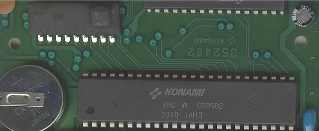
This is the VRC7 portion of the Lagrange Point PCB. In clockwise order: 1) The OPLL post-processor (as the YM2413's (and derrivatives) output is raw), 2) The VRC7, and 3) The SRAM battery, which is there for no reason whatsoever as it only has relevance to SRAM. This image was scanned by myself, and I upload it without a license for all to use. |
| Date | 31 May 2007 (original upload date) |
| Source | Transferred from en.wikipedia to Commons. |
| Author | UNKNOWNFILE at English Wikipedia |
Licensing
| This work has been released into the
public domain by its author,
UNKNOWNFILE at
English Wikipedia. This applies worldwide. In some countries this may not be legally possible; if so: UNKNOWNFILE grants anyone the right to use this work for any purpose, without any conditions, unless such conditions are required by law. |
Original upload log
- 2007-05-31 21:43 UNKNOWNFILE 1425×588×8 (45344 bytes) fixing color levels
- 2007-05-31 21:38 UNKNOWNFILE 1425×588×8 (51784 bytes) This is the VRC7 portion of the Lagrange Point PCB. In clockwise order: 1) The OPLL post-processor (as the YM2413's (and derrivatives) output is raw), 2) The VRC7, and 3) The SRAM battery, which is there for no reason whatsoever as it only has relevanc
File history
Click on a date/time to view the file as it appeared at that time.
| Date/Time | Thumbnail | Dimensions | User | Comment | |
|---|---|---|---|---|---|
| current | 11:26, 25 September 2007 |
| 1,425 × 588 (44 KB) | Liftarn | {{Information |Description=This is the VRC7 portion of the Lagrange Point PCB. In clockwise order: 1) The OPLL post-processor (as the YM2413's (and derrivatives) output is raw), 2) The VRC7, and 3) The SRAM battery, which is there for no reason whatsoe |
File usage
Global file usage
The following other wikis use this file:
- Usage on es.wikipedia.org
- Usage on fr.wikipedia.org
- Usage on it.wikipedia.org
Metadata
Original file (1,425 × 588 pixels, file size: 44 KB, MIME type: image/jpeg)
| This is a file from the
Wikimedia Commons. Information from its
description page there is shown below. Commons is a freely licensed media file repository. You can help. |
Summary
| Description |
This is the VRC7 portion of the Lagrange Point PCB. In clockwise order: 1) The OPLL post-processor (as the YM2413's (and derrivatives) output is raw), 2) The VRC7, and 3) The SRAM battery, which is there for no reason whatsoever as it only has relevance to SRAM. This image was scanned by myself, and I upload it without a license for all to use. |
| Date | 31 May 2007 (original upload date) |
| Source | Transferred from en.wikipedia to Commons. |
| Author | UNKNOWNFILE at English Wikipedia |
Licensing
| This work has been released into the
public domain by its author,
UNKNOWNFILE at
English Wikipedia. This applies worldwide. In some countries this may not be legally possible; if so: UNKNOWNFILE grants anyone the right to use this work for any purpose, without any conditions, unless such conditions are required by law. |
Original upload log
- 2007-05-31 21:43 UNKNOWNFILE 1425×588×8 (45344 bytes) fixing color levels
- 2007-05-31 21:38 UNKNOWNFILE 1425×588×8 (51784 bytes) This is the VRC7 portion of the Lagrange Point PCB. In clockwise order: 1) The OPLL post-processor (as the YM2413's (and derrivatives) output is raw), 2) The VRC7, and 3) The SRAM battery, which is there for no reason whatsoever as it only has relevanc
File history
Click on a date/time to view the file as it appeared at that time.
| Date/Time | Thumbnail | Dimensions | User | Comment | |
|---|---|---|---|---|---|
| current | 11:26, 25 September 2007 |
| 1,425 × 588 (44 KB) | Liftarn | {{Information |Description=This is the VRC7 portion of the Lagrange Point PCB. In clockwise order: 1) The OPLL post-processor (as the YM2413's (and derrivatives) output is raw), 2) The VRC7, and 3) The SRAM battery, which is there for no reason whatsoe |
File usage
Global file usage
The following other wikis use this file:
- Usage on es.wikipedia.org
- Usage on fr.wikipedia.org
- Usage on it.wikipedia.org